-
LM3488/-Q1 Automotive High-Efficiency Controller for Boost, SEPIC and Fly-Back DC-DC Converters
- 1 Features
- 2 Applications
- 3 Description
- 4 Revision History
- 5 Pin Configuration and Functions
- 6 Specifications
- 7 Detailed Description
-
8 Application and Implementation
- 8.1 Application Information
- 8.2
Typical Applications
- 8.2.1
Boost Converter
- 8.2.1.1 Design Requirements
- 8.2.1.2
Detailed Design Procedure
- 8.2.1.2.1 Custom Design with WEBENCH Tools
- 8.2.1.2.2 Power Inductor Selection
- 8.2.1.2.3 Programming the Output Voltage
- 8.2.1.2.4 Setting the Current Limit
- 8.2.1.2.5 Current Limit with External Slope Compensation
- 8.2.1.2.6 Power Diode Selection
- 8.2.1.2.7 Power MOSFET Selection
- 8.2.1.2.8 Input Capacitor Selection
- 8.2.1.2.9 Output Capacitor Selection
- 8.2.1.3 Application Curve
- 8.2.2 Designing SEPIC Using LM3488
- 8.2.1
Boost Converter
- 9 Power Supply Recommendations
- 10Layout
- 11Device and Documentation Support
- 12Mechanical, Packaging, and Orderable Information
- IMPORTANT NOTICE
Package Options
Mechanical Data (Package|Pins)
- DGK|8
Thermal pad, mechanical data (Package|Pins)
Orderable Information
LM3488/-Q1 Automotive High-Efficiency Controller for Boost, SEPIC and Fly-Back DC-DC Converters
1 Features
- Automotive Grade Product, AEC-Q100 Qualified
- 8-Lead VSSOP Package
- Internal Push-Pull Driver With 1-A Peak Current Capability
- Current Limit and Thermal Shutdown
- Frequency Compensation Optimized With a Capacitor and a Resistor
- Internal Soft-Start
- Current Mode Operation
- Undervoltage Lockout With Hysteresis
- Key Specifications:
- Wide Supply Voltage Range of 2.97 V to 40 V
- 100-kHz to 1-MHz Adjustable and Synchronizable Clock Frequency
- ±1.5% (Overtemperature) Internal Reference
- 5-µA Shutdown Current (Overtemperature)
- Create a Custom Design Using the LM3488 with the WEBENCH Power Designer
2 Applications
3 Description
The LM3488 is a versatile low-side N-FET high-performance controller for switching regulators. This device is suitable for use in topologies requiring low-side FET, such as boost, flyback, or SEPIC. Moreover, the LM3488 can be operated at extremely high switching frequency to reduce the overall solution size. The switching frequency of LM3488 can be adjusted to any value from 100 kHz to 1 MHz by using a single external resistor or by synchronizing it to an external clock. Current mode control provides superior bandwidth and transient response, besides cycle-by-cycle current limiting. Output current can be programmed with a single external resistor.
The LM3488 has built-in features such as thermal shutdown, short-circuit protection, and overvoltage protection. Power-saving shutdown mode reduces the total supply current to 5 µA and allows power supply sequencing. Internal soft-start limits the inrush current at start-up.
Device Information(1)
| PART NUMBER | PACKAGE | BODY SIZE (NOM) |
|---|---|---|
| LM3488 | VSSOP (8) | 3.00 mm × 3.00 mm |
| LM3488-Q1 |
- For all available packages, see the orderable addendum at the end of the datasheet.
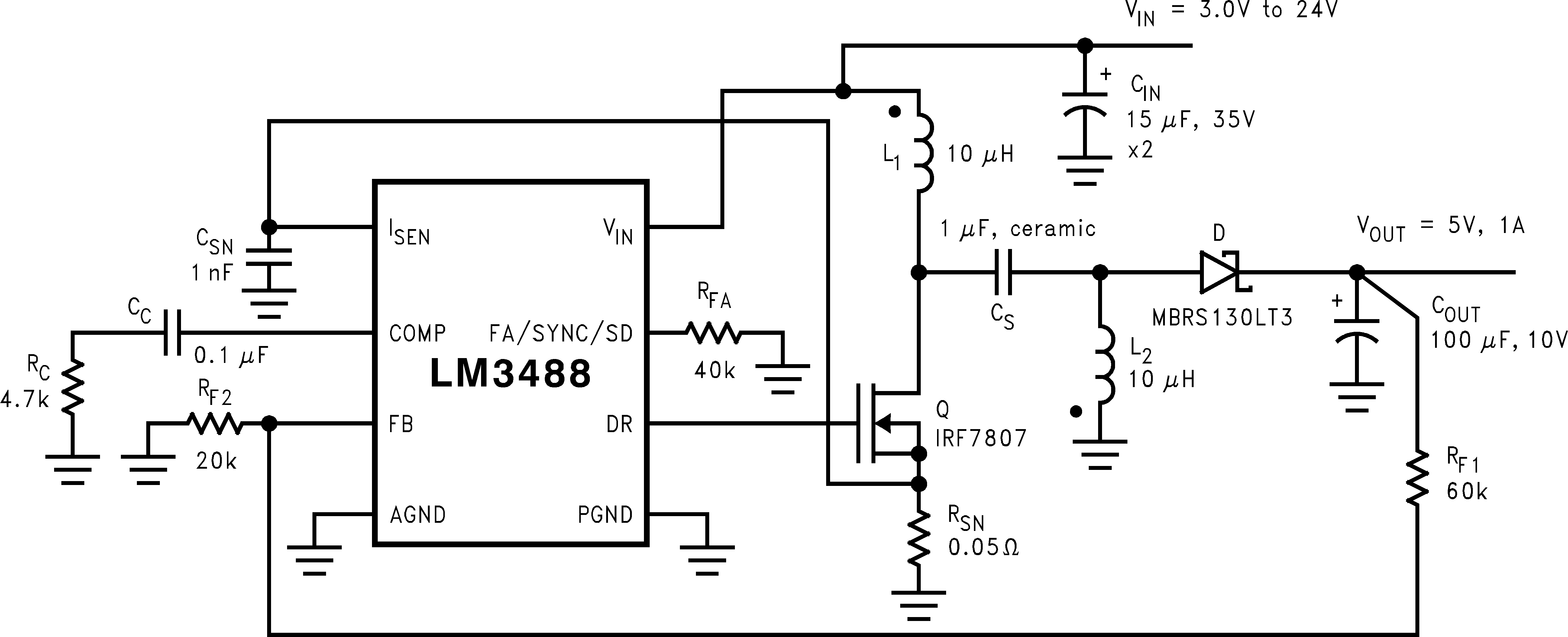
Typical SEPIC Converter
4 Revision History
Changes from N Revision (December 2014) to O Revision
Changes from M Revision (March 2013) to N Revision
- Added Pin Configuration and Functions section, Handling Rating table, Feature Description section, Device Functional Modes, Application and Implementation section, Power Supply Recommendations section, Layout section, Device and Documentation Support section, and Mechanical, Packaging, and Orderable Information section Go
- Changed ESD Table and Features sectionGo
- Changed application information. Go
Changes from L Revision (March 2013) to M Revision
- Changed layout of National Data Sheet to TI format Go
5 Pin Configuration and Functions

Pin Functions
| PIN | TYPE | DESCRIPTION | |
|---|---|---|---|
| NAME | NO. | ||
| ISEN | 1 | I | Current sense input pin. Voltage generated across an external sense resistor is fed into this pin. |
| COMP | 2 | A | Compensation pin. A resistor, capacitor combination connected to this pin provides compensation for the control loop. |
| FB | 3 | I | Feedback pin. The output voltage should be adjusted using a resistor divider to provide 1.26 V at this pin. |
| AGND | 4 | P | Analog ground pin. |
| PGND | 5 | P | Power ground pin. |
| DR | 6 | O | Drive pin of the IC. The gate of the external MOSFET should be connected to this pin. |
| FA/SYNC/SD | 7 | A | Frequency adjust, synchronization, and Shutdown pin. A resistor connected to this pin sets the oscillator frequency. An external clock signal at this pin will synchronize the controller to the frequency of the clock. A high level on this pin for ≥ 30 µs will turn the device off. The device will then draw less than 10µA from the supply. |
| VIN | 8 | P | Power supply input pin. |
6 Specifications
6.1 Absolute Maximum Ratings (1)
| MIN | MAX | UNIT | ||
|---|---|---|---|---|
| Input voltage | 45 | V | ||
| FB pin voltage | –0.4 < VFB | VFB < 7 | V | |
| FA/SYNC/SD pin voltage | –0.4 < VFA/SYNC/SD | VFA/SYNC/SD < 7 | V | |
| Peak driver output current (< 10 µs) | 1 | A | ||
| Power dissipation | Internally Limited | |||
| Junction temperature | 150 | °C | ||
| Lead temperature | Vapor Phase (60 s) | 215 | °C | |
| Infared (15 s) | 260 | °C | ||
| DR pin voltage | −0.4 ≤ VDR | VDR ≤ 8 | V | |
| ILIM pin voltage | 600 | mV | ||
6.2 ESD Ratings : LM3488
| MIN | MAX | UNIT | |||
|---|---|---|---|---|---|
| V(ESD) | Electrostatic discharge | Human body model (HBM), per ANSI/ESDA/JEDEC JS-001, all pins(1) | –2000 | 2000 | V |
| Charged device model (CDM), per JEDEC specification JESD22-C101, all pins(2) | –750 | 750 | |||
6.3 ESD Ratings: LM3488-Q1
| MIN | MAX | UNIT | ||||
|---|---|---|---|---|---|---|
| V(ESD) | Electrostatic discharge | Human body model (HBM), per AEC Q100-002(1) | –2000 | 2000 | V | |
| Charged device model (CDM), per AEC Q100-011 | Corner pins (1, 4, 5, and 8) | –750 | 750 | |||
| Other pins | –750 | 750 | ||||
6.4 Recommended Operating Conditions
| MIN | MAX | UNIT | |
|---|---|---|---|
| Supply Voltage | 2.97 ≤ VIN | VIN ≤ 40 | V |
| Junction Temperature Range | −40 ≤ TJ | TJ ≤ 125 | °C |
| Switching Frequency | 100 ≤ FSW | FSW ≤ 1 | kHz/MHz |
6.5 Thermal Information
| THERMAL METRIC(1) | LM3488, LM3488-Q1 |
UNIT | |
|---|---|---|---|
| DGK | |||
| 8 PINS | |||
| RθJA | Junction-to-ambient thermal resistance | 160 | °C/W |
| RθJC(top) | Junction-to-case (top) thermal resistance | 50 | |
| RθJB | Junction-to-board thermal resistance | 77 | |
| ψJT | Junction-to-top characterization parameter | 4.7 | |
| ψJB | Junction-to-board characterization parameter | 76 | |
6.6 Electrical Characteristics
Unless otherwise specified, VIN = 12 V, RFA = 40 kΩ, TJ = 25°C| PARAMETER | TEST CONDITIONS | MIN | TYP | MAX | UNIT | |
|---|---|---|---|---|---|---|
| VFB | Feedback Voltage | VCOMP = 1.4 V, 2.97 ≤ VIN ≤ 40 V | 1.2507 | 1.26 | 1.2753 | V |
| VCOMP = 1.4 V, 2.97 ≤ VIN ≤ 40 V, −40°C ≤ TJ ≤ 125°C | 1.24 | 1.28 | ||||
| ΔVLINE | Feedback Voltage Line Regulation | 2.97 ≤ VIN ≤ 40 V | 0.001 | %/V | ||
| ΔVLOAD | Output Voltage Load Regulation | IEAO Source/Sink | ±0.5 | %/V (max) | ||
| VUVLO | Input Undervoltage Lock-out | 2.85 | V | |||
| −40°C ≤ TJ ≤ 125°C | 2.97 | |||||
| VUV(HYS) | Input Undervoltage Lock-out Hysteresis | 170 | mV | |||
| −40°C ≤ TJ ≤ 125°C | 130 | 210 | ||||
| Fnom | Nominal Switching Frequency | RFA = 40 KΩ | 400 | kHz | ||
| RFA = 40 KΩ, −40°C ≤ TJ ≤ 125°C | 360 | 430 | ||||
| RDS1 (ON) | Driver Switch On Resistance (top) | IDR = 0.2A, VIN= 5 V | 16 | Ω | ||
| RDS2 (ON) | Driver Switch On Resistance (bottom) | IDR = 0.2A | 4.5 | Ω | ||
| VDR (max) | Maximum Drive Voltage Swing(3) | VIN < 7.2 V | VIN | V | ||
| VIN ≥ 7.2 V | 7.2 | |||||
| Dmax | Maximum Duty Cycle(4) | 100% | ||||
| Tmin (on) | Minimum On Time | 325 | nsec | |||
| −40°C ≤ TJ ≤ 125°C | 230 | 550 | ||||
| ISUPPLY | Supply Current (switching) | See (6) | 2.7 | mA | ||
| See (6), −40°C ≤ TJ ≤ 125°C | 3.0 | |||||
| IQ | Quiescent Current in Shutdown Mode | VFA/SYNC/SD = 5 V(7), VIN = 5 V | 5 | µA | ||
| VFA/SYNC/SD = 5 V(7), VIN = 5 V, −40°C ≤ TJ ≤ 125°C | 7 | |||||
| VSENSE | Current Sense Threshold Voltage | VIN = 5 V | 135 | 156 | 180 | mV |
| VIN = 5 V, −40°C ≤ TJ ≤ 125°C | 125 | 190 | ||||
| VSC | Short-Circuit Current Limit Sense Voltage | VIN = 5 V | 343 | mV | ||
| VIN = 5 V, −40°C ≤ TJ ≤ 125°C | 250 | 415 | ||||
| VSL | Internal Compensation Ramp Voltage | VIN = 5 V | 92 | mV | ||
| VIN = 5 V, −40°C ≤ TJ ≤ 125°C | 52 | 132 | ||||
| VSL ratio | VSL/VSENSE | 0.30 | 0.49 | 0.70 | ||
| VOVP | Output Overvoltage Protection (with respect to feedback voltage) (5) | VCOMP = 1.4 V | 32 | 50 | 78 | mV |
| VCOMP = 1.4 V, −40°C ≤ TJ ≤ 125°C | 25 | 85 | ||||
| VOVP(HYS) | Output Over-Voltage Protection Hysteresis(5) | VCOMP = 1.4 V | 60 | mV | ||
| VCOMP = 1.4 V, −40°C ≤ TJ ≤ 125°C | 20 | 110 | ||||
| Gm | Error Ampifier Transconductance | VCOMP = 1.4 V, IEAO = 100 µA (Source/Sink) | 600 | 800 | 1000 | µmho |
| VCOMP = 1.4 V, IEAO = 100 µA (Source/Sink), −40°C ≤ TJ ≤ 125°C | 365 | 1265 | ||||
| AVOL | Error Amplifier Voltage Gain | VCOMP = 1.4 V, IEAO = 100 µA (Source/Sink) | 38 | V/V | ||
| VCOMP = 1.4 V, IEAO = 100 µA (Source/Sink), −40°C ≤ TJ ≤ 125°C | 26 | 44 | ||||
| IEAO | Error Amplifier Output Current (Source/ Sink) | Source, VCOMP = 1.4 V, VFB = 0 V | 80 | 110 | 140 | µA |
| Source, VCOMP = 1.4 V, VFB = 0 V, −40°C ≤ TJ ≤ 125°C | 50 | 180 | ||||
| Sink, VCOMP = 1.4 V, VFB = 1.4 V | −100 | −140 | −180 | µA | ||
| Sink, VCOMP = 1.4 V, VFB = 1.4 V, −40°C ≤ TJ ≤ 125°C | −85 | −185 | ||||
| VEAO | Error Amplifier Output Voltage Swing | Upper Limit: VFB = 0 V, COMP Pin = Floating | 2.2 | V | ||
| Upper Limit: VFB = 0 V, COMP Pin = Floating, −40°C ≤ TJ ≤ 125°C | 1.8 | 2.4 | ||||
| Lower Limit: VFB = 1.4 V | 0.56 | V | ||||
| Lower Limit: VFB = 1.4 V, −40°C ≤ TJ ≤ 125°C | 0.2 | 1.0 | ||||
| TSS | Internal Soft-Start Delay | VFB = 1.2 V, VCOMP = Floating | 4 | ms | ||
| Tr | Drive Pin Rise Time | Cgs = 3000 pf, VDR = 0 to 3 V | 25 | ns | ||
| Tf | Drive Pin Fall Time | Cgs = 3000 pf, VDR = 0 to 3 V | 25 | ns | ||
| VSD | Shutdown and Synchronization signal threshold (2) | Output = High | 1.27 | V | ||
| Output = High, −40°C ≤ TJ ≤ 125°C | 1.4 | |||||
| Output = Low | 0.65 | V | ||||
| Output = Low, −40°C ≤ TJ ≤ 125°C | 0.3 | |||||
| ISD | Shutdown Pin Current | VSD = 5 V | −1 | µA | ||
| VSD = 0 V | +1 | |||||
| IFB | Feedback Pin Current | 15 | nA | |||
| TSD | Thermal Shutdown | 165 | °C | |||
| Tsh | Thermal Shutdown Hysteresis | 10 | °C |
6.7 Typical Characteristics
Unless otherwise specified, VIN = 12V, TJ = 25°C.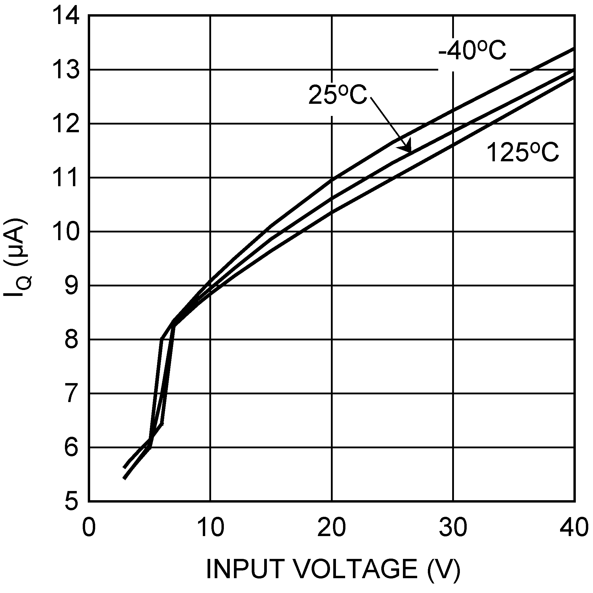 Figure 1. IQ vs Temperature & Input Voltage
 Figure 3. ISupply vs VIN
 Figure 5. Frequency vs Temperature
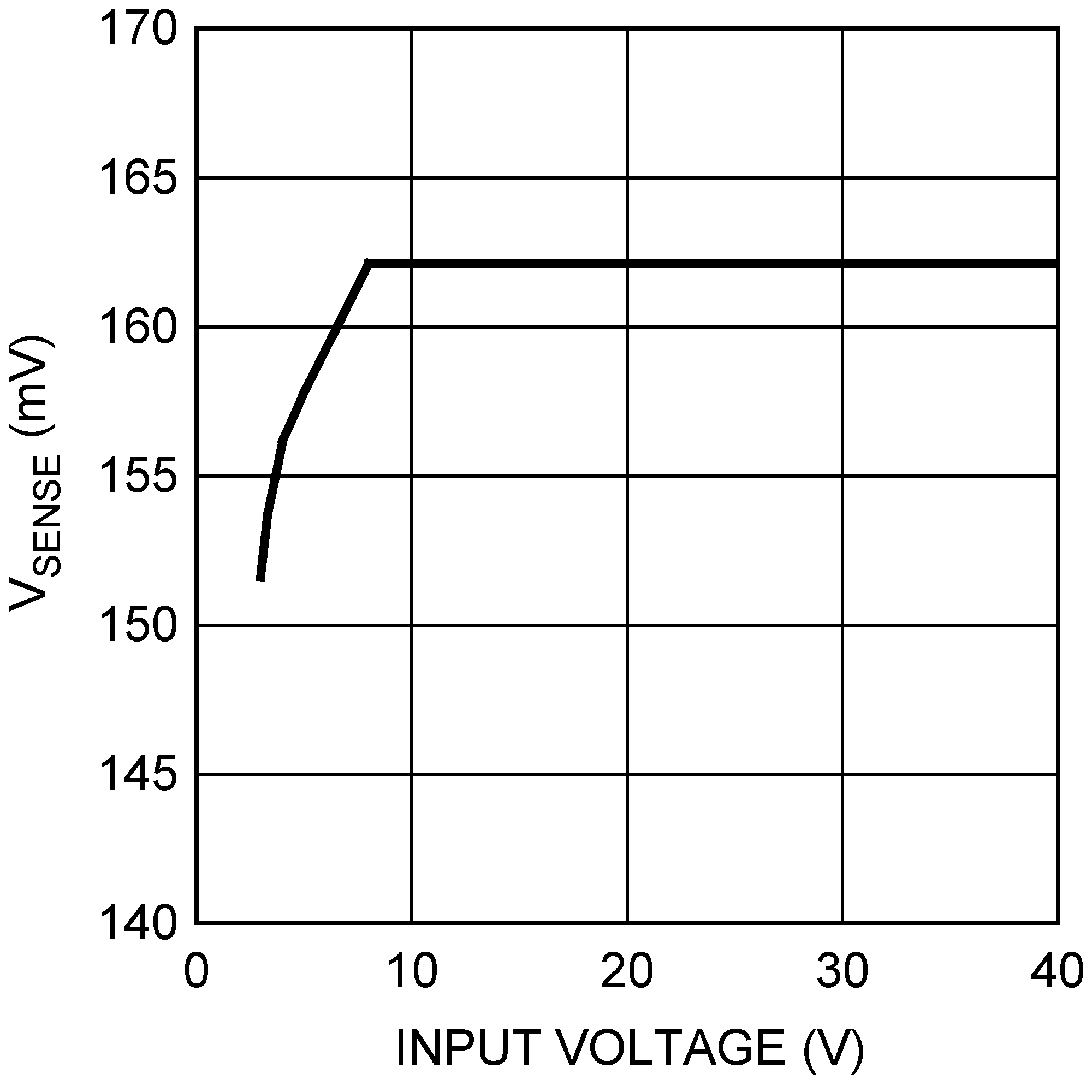 Figure 7. Current Sense Threshold vs Input Voltage
 Figure 9. Efficiency vs Load Current (3.3 V In and 12 V Out)
 Figure 11. Efficiency vs Load Current (9 V In and 12 V Out)
 Figure 13. Error Amplifier Gain
 Figure 15. COMP Pin Source Current vs Temperature
 Figure 17. Compensation Ramp vs Compensation Resistor
 Figure 19. Current Sense Voltage vs Duty Cycle
 Figure 2. ISupply vs Input Voltage (Non-Switching)
 Figure 4. Switching Frequency vs RFA
 Figure 6. Drive Voltage vs Input Voltage
 Figure 8. COMP Pin Voltage vs Load Current
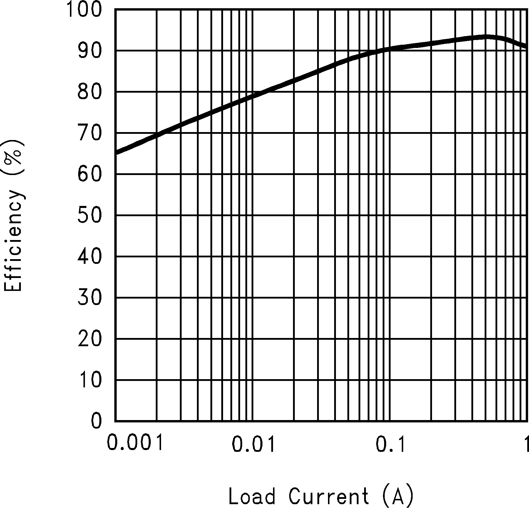 Figure 10. Efficiency vs Load Current (5 V In and 12 V Out)
 Figure 12. Efficiency vs Load Current (3.3 V In and 5 V Out)
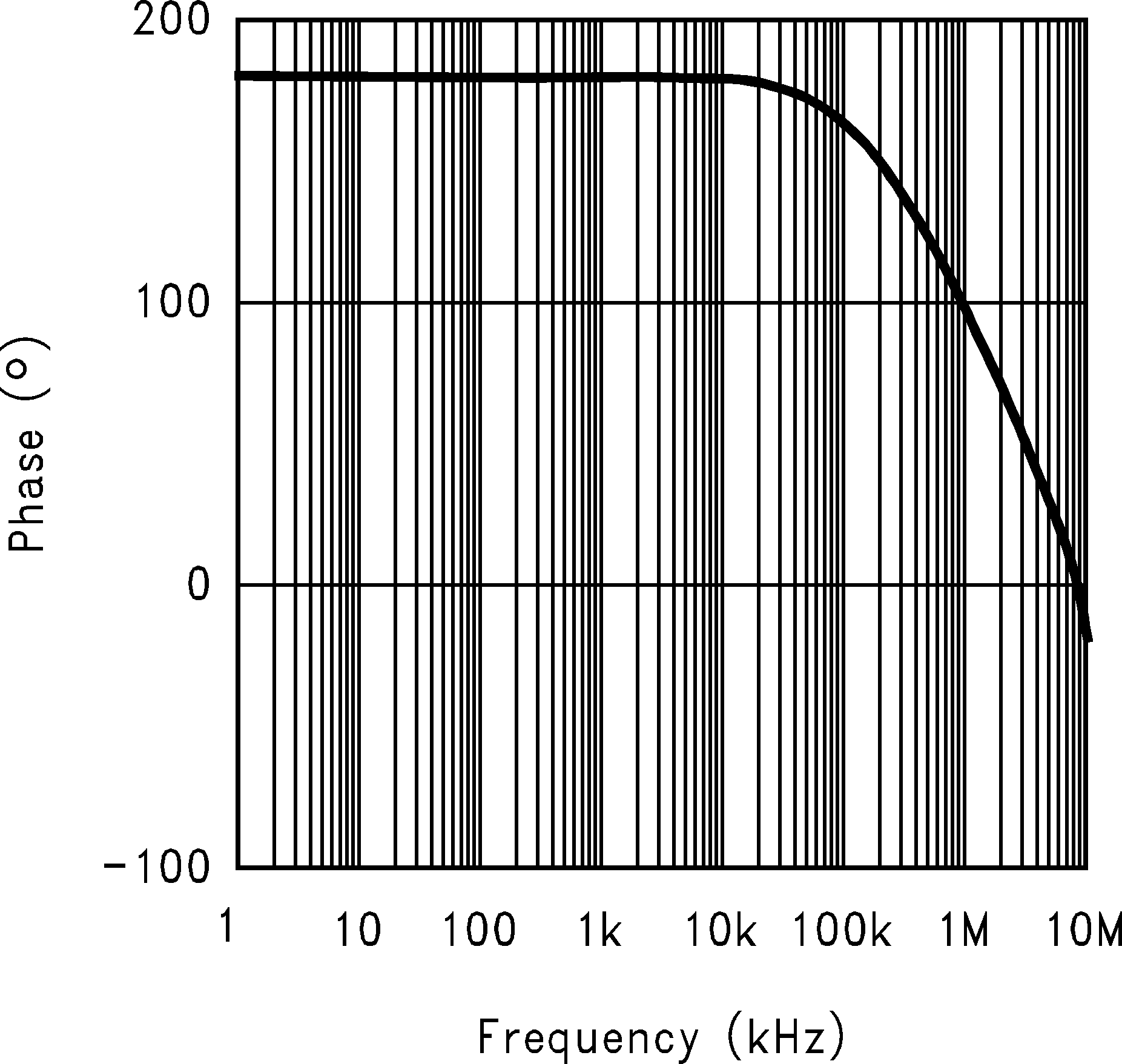 Figure 14. Error Amplifier Phase
 Figure 16. Short Circuit Protection vs Input Voltage
 Figure 18. Shutdown Threshold Hysteresis vs Temperature
7 Detailed Description
7.1 Overview
The LM3488 uses a fixed frequency, Pulse Width Modulated (PWM), current mode control architecture. In a typical application circuit, the peak current through the external MOSFET is sensed through an external sense resistor. The voltage across this resistor is fed into the ISEN pin. This voltage is then level shifted and fed into the positive input of the PWM comparator. The output voltage is also sensed through an external feedback resistor divider network and fed into the error amplifier negative input (feedback pin, FB). The output of the error amplifier (COMP pin) is added to the slope compensation ramp and fed into the negative input of the PWM comparator.
At the start of any switching cycle, the oscillator sets the RS latch using the SET/Blank-out and switch logic blocks. This forces a high signal on the DR pin (gate of the external MOSFET) and the external MOSFET turns on. When the voltage on the positive input of the PWM comparator exceeds the negative input, the RS latch is reset and the external MOSFET turns off.
The voltage sensed across the sense resistor generally contains spurious noise spikes, as shown in Figure 20. These spikes can force the PWM comparator to reset the RS latch prematurely. To prevent these spikes from resetting the latch, a blank-out circuit inside the IC prevents the PWM comparator from resetting the latch for a short duration after the latch is set. This duration is about 150ns and is called the blank-out time.
Under extremely light load or no-load conditions, the energy delivered to the output capacitor when the external MOSFET is on during the blank-out time is more than what is delivered to the load. An over-voltage comparator inside the LM3488 prevents the output voltage from rising under these conditions. The over-voltage comparator senses the feedback (FB pin) voltage and resets the RS latch under these conditions. The latch remains in reset state till the output decays to the nominal value.
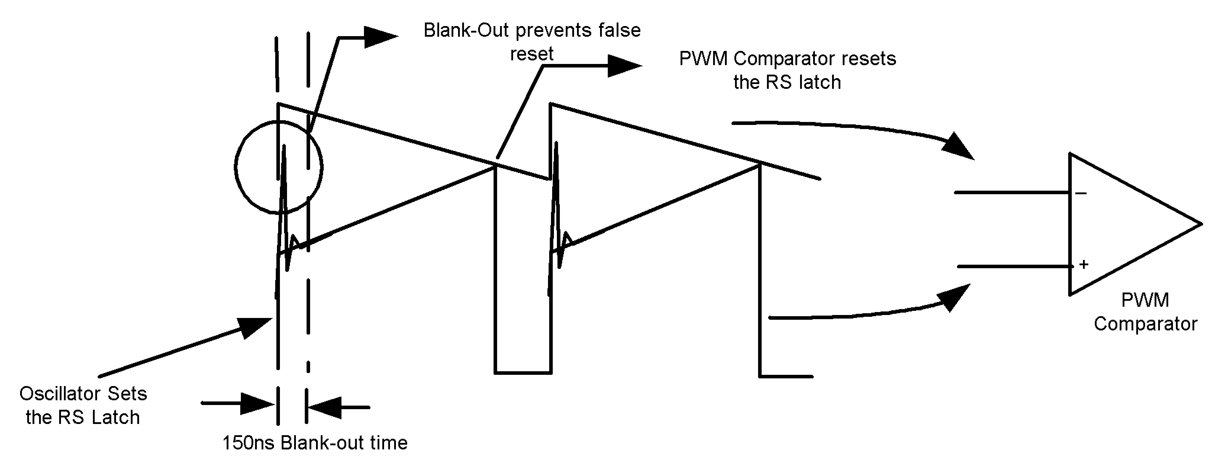 Figure 20. Basic Operation of the PWM Comparator
7.2 Functional Block Diagram

7.3 Feature Description
7.3.1 Slope Compensation Ramp
The LM3488 uses a current mode control scheme. The main advantages of current mode control are inherent cycle-by-cycle current limit for the switch, and simpler control loop characteristics. It is also easy to parallel power stages using current mode control since as current sharing is automatic.
Current mode control has an inherent instability for duty cycles greater than 50%, as shown in Figure 21. In Figure 21, a small increase in the load current causes the switch current to increase by ΔIO. The effect of this load change, ΔI1, is :

From the above equation, when D > 0.5, ΔI1 will be greater than ΔIO. In other words, the disturbance is divergent. So a very small perturbation in the load will cause the disturbance to increase.
To prevent the sub-harmonic oscillations, a compensation ramp is added to the control signal, as shown in Figure 22.
With the compensation ramp,

 Figure 21. Sub-Harmonic Oscillation for D>0.5
 Figure 22. Compensation Ramp Avoids Sub-Harmonic Oscillation
The compensation ramp has been added internally in LM3488. The slope of this compensation ramp has been selected to satisfy most of the applications. The slope of the internal compensation ramp depends on the frequency. This slope can be calculated using the formula:
In the above equation, VSL is the amplitude of the internal compensation ramp. Limits for VSL have been specified in the electrical characteristics.
In order to provide the user additional flexibility, a patented scheme has been implemented inside the IC to increase the slope of the compensation ramp externally, if the need arises. Adding a single external resistor, RSL(as shown in Figure 23) increases the slope of the compensation ramp, MC by :

In this equation, ΔVSL is equal to 40.10-6RSL. Hence,

ΔVSL versus RSL has been plotted in Figure 24 for different frequencies.
 Figure 23. Increasing the Slope of the Compensation Ramp
 Figure 24. ΔVSL vs RSL
7.3.2 Frequency Adjust/Synchronization/Shutdown
The switching frequency of LM3488 can be adjusted between 100kHz and 1MHz using a single external resistor. This resistor must be connected between FA/SYNC/SD pin and ground, as shown in Figure 25. See Typical Characteristics to determine the value of the resistor required for a desired switching frequency.
The LM3488 can be synchronized to an external clock. The external clock must be connected to the FA/SYNC/SD pin through a resistor, RSYNC as shown in Figure 26. The value of this resistor is dependent on the off time of the synchronization pulse, TOFF(SYNC). Table 1 shows the range of resistors to be used for a given TOFF(SYNC).
Table 1. Recommended Series Resistance for Synchronization
| TOFF(SYNC) (µs) | RSYNC range (kΩ) |
|---|---|
| 1 | 5 to 13 |
| 2 | 20 to 40 |
| 3 | 40 to 65 |
| 4 | 55 to 90 |
| 5 | 70 to 110 |
| 6 | 85 to 140 |
| 7 | 100 to 160 |
| 8 | 120 to 190 |
| 9 | 135 to 215 |
| 10 | 150 to 240 |
It is also necessary to have the width of the synchronization pulse wider than the duty cycle of the converter (when DR pin is high and the switching point is low). It is also necessary to have the synchronization pulse width ≥ 300nsecs.
The FA/SYNC/SD pin also functions as a shutdown pin. If a high signal (see Electrical Characteristics for definition of high signal) appears on the FA/SYNC/SD pin, the LM3488 stops switching and goes into a low current mode. The total supply current of the IC reduces to less than 10µA under these conditions.
Figure 27 and Figure 28 show implementation of shutdown function when operating in Frequency adjust mode and synchronization mode respectively. In frequency adjust mode, connecting the FA/SYNC/SD pin to ground forces the clock to run at a certain frequency. Pulling this pin high shuts down the IC. In frequency adjust or synchronization mode, a high signal for more than 30µs shuts down the IC.
Figure 29 shows implementation of both frequency adjust with RFA resistor and frequency synchronization with RSYNC. The switching frequency is defined by RFA when a synchronization signal is not applied. When sync is applied it overrides the RFA setting.
 Figure 25. Frequency Adjust
 Figure 26. Frequency Synchronization
 Figure 27. Shutdown Operation in Frequency Adjust Mode
 Figure 28. Shutdown Operation in Synchronization Mode
 Figure 29. Frequency Adjust or Frequency Synchronization
7.3.3 Short-Circuit Protection
When the voltage across the sense resistor (measured on ISEN Pin) exceeds 350mV, short-circuit current limit gets activated. A comparator inside LM3488 reduces the switching frequency by a factor of 5 and maintains this condition till the short is removed.
7.4 Device Functional Modes
The device is set to run as soon as the input voltage crosses above the UVLO set point and at a frequency set according to the FA/SYNC/SD pin pull-down resistor or to run at a frequency set by the waveform applied to the FA/SYNC/SD pin.
If the FA/SYNC/SD pin is pulled high, the LM3488 enters shut-down mode.
If the voltage at the ISEN pin exceeds Vsc, the device enters short-circuit protection mode.