SNVS598B August 2010 – March 2018 LM3535
PRODUCTION DATA.
- 1 Features
- 2 Applications
- 3 Description
- 4 Revision History
- 5 Pin Configuration and Functions
- 6 Specifications
- 7 Detailed Description
-
8 Application and Implementation
- 8.1 Application Information
- 8.2
Typical Application
- 8.2.1 Design Requirements
- 8.2.2 Detailed Design Procedure
- 8.2.3 Application Curves
- 9 Power Supply Recommendations
- 10Layout
- 11Device and Documentation Support
- 12Mechanical, Packaging, and Orderable Information
Package Options
Mechanical Data (Package|Pins)
- YFQ|20
Thermal pad, mechanical data (Package|Pins)
Orderable Information
8.2.2.1.2 ALS Operation
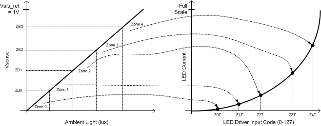
The ambient light sensor input has a 0 to 1 V operational input voltage range. The Specifications shows the LM3535 with an ambient light sensor (AVAGO, APDS-9005) and the internal ALS Resistor Select Register set to 0x40 (2.32 kΩ). This circuit converts 0 to 1000 LUX light into approximately a 0 to 850 mV linear output voltage. The voltage at the active ambient light sensor input is compared against the 8 bit values programmed into the Zone Boundary Registers (ZB0-ZB3). When the ambient light sensor output crosses one of the ZB0 – ZB3 programmed thresholds the internal ALS circuitry will smoothly transition the LED current to the new 7 bit brightness level as programmed into the appropriate Zone Target Register (Z0T – Z4T, see Figure 28).
With bits [6:4] of the Configuration Register set to 1 (Bit6 = ALS Block Enable, Bit5 = BankB ALS Enable, Bit4 = BankA ALS Enable), the LM3535 is configured for ambient light current Control. In this mode the ambient light sensing input (ALS) monitors the output of analog output ambient light sensing photo diode and adjusts the LED current depending on the ambient light. The ambient light sensing circuit has 4 configurable ambient light boundaries (ZB0 – ZB3) programmed through the four (8-bit) Zone Boundary Registers. These zone boundaries define 5 ambient brightness zones.
On start-up the 4 Zone Boundary Registers are pre-loaded with 0x33 (51d), 0x66 (102d), 0x99 (153d), and 0xCC (204d). The ALS input has a 1-V active input voltage range which makes the default Zone Boundaries approx. set at:
Zone Boundary 0 = 200 mV
Zone Boundary 1 = 400 mV
Zone Boundary 2 = 600 mV
Zone Boundary 3 = 800 mV
These Zone Boundary Registers are all 8-bit (readable and writable) registers. By default, the first zone (Z0) is defined between 0 and 200 mV, default for Z1 is defined between 200 mV and 400 mV, Z2 is defined between 400 mV and 600 mV, Z3 is defined between 600 mV and 800 mV, and Z4 is defined between 800 mV and 1 V. The default settings for the 5 Zone Target Registers are 0x19, 0x33, 0x4C, 0x66, and 0x7F. This corresponds to LED brightness settings of 84 µA, 164 µA, 1.45 mA, 6.17 mA and 25 mA of current, respectively. See Figure 31.
 Figure 31. ALS Zone to LED Brightness Mapping