SNVS598B August 2010 – March 2018 LM3535
PRODUCTION DATA.
- 1 Features
- 2 Applications
- 3 Description
- 4 Revision History
- 5 Pin Configuration and Functions
- 6 Specifications
- 7 Detailed Description
-
8 Application and Implementation
- 8.1 Application Information
- 8.2
Typical Application
- 8.2.1 Design Requirements
- 8.2.2 Detailed Design Procedure
- 8.2.3 Application Curves
- 9 Power Supply Recommendations
- 10Layout
- 11Device and Documentation Support
- 12Mechanical, Packaging, and Orderable Information
Package Options
Mechanical Data (Package|Pins)
- YFQ|20
Thermal pad, mechanical data (Package|Pins)
Orderable Information
5 Pin Configuration and Functions
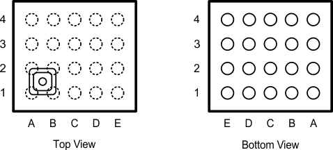
YFQ Package
20-Pin DSBGA
Top View

Pin Functions
| PIN | TYPE | DESCRIPTION | |
|---|---|---|---|
| NO. | NAME | ||
| A1, C1, B1, B2 | C1+, C1–, C2+, C2– | Power | Flying capacitor connections |
| A2 | VOUT | Power | Charge pump output voltage |
| A3 | VIN | Power | Input voltage; input range: 2.7 V to 5.5 V |
| A4 | GND | Power | Ground |
| B3 | D1B / INT | Input / Output | LED driver/ ALS interrupt - GroupB current sink or ALS interrupt pin. In ALS Interrupt mode, a pullup resistor is required. A zero (0) means a change has occurred, while a one (1) means no ALS adjustment has been made. |
| B4, C4 | D53, D62 | Output | LED drivers - configurable current sinks. Can be assigned to GroupA or GroupB |
| C2 | SDIO | Input / Output | Serial data input/output pin |
| C3 | D1C / ALS | Input / Output | LED driver / ALS input - indicator LED current sink or ambient light sensor input |
| D1 | GND | Power | Ground |
| D2 | PWM | Input | External PWM input - allows the current sinks to be turned on and off at a frequency and duty cycle externally controlled. Minimum on-time pulse width = 15 µsec. |
| D3, E3, E4, D4 | D1A-D4A | Output | LED drivers - GroupA |
| E1 | HWEN | Input | Hardware enable pin. High = normal operation, Low = RESET |
| E2 | SCL | Input | Serial clock pin |