SNVS598B August   2010  – March 2018 LM3535

PRODUCTION DATA.  

  1. Features
  2. Applications
  3. Description
    1.     Device Images
      1.      Typical Application
  4. Revision History
  5. Pin Configuration and Functions
    1.     Pin Functions
  6. Specifications
    1. 6.1 Absolute Maximum Ratings
    2. 6.2 ESD Ratings
    3. 6.3 Recommended Operating Conditions
    4. 6.4 Thermal Information
    5. 6.5 Electrical Characteristics
    6. 6.6 Typical Characteristics
  7. Detailed Description
    1. 7.1 Overview
    2. 7.2 Functional Block Diagram
    3. 7.3 Feature Description
      1. 7.3.1 Charge Pump
      2. 7.3.2 Diode Current Sinks
      3. 7.3.3 Ambient Light Sensing (ALS) And Interrupt
      4. 7.3.4 Dynamic Backlight Control Input (PWM Pin)
      5. 7.3.5 LED Forward Voltage Monitoring
      6. 7.3.6 Configurable Gain Transition Delay
      7. 7.3.7 Hardware Enable (HWEN)
    4. 7.4 Device Functional Modes
      1. 7.4.1 Shutdown
      2. 7.4.2 Standby
      3. 7.4.3 Active Mode
    5. 7.5 Programming
      1. 7.5.1 I2C Compatible Interface
        1. 7.5.1.1 Data Validity
        2. 7.5.1.2 Start and Stop Conditions
        3. 7.5.1.3 Transferring Data
        4. 7.5.1.4 I2C Compatible Chip Address
        5. 7.5.1.5 Internal Registers of LM3535
  8. Application and Implementation
    1. 8.1 Application Information
    2. 8.2 Typical Application
      1. 8.2.1 Design Requirements
      2. 8.2.2 Detailed Design Procedure
        1. 8.2.2.1 Ambient Light Sensing
          1. 8.2.2.1.1 Ambient Light Sensor Block
          2. 8.2.2.1.2 ALS Operation
            1. 8.2.2.1.2.1 ALS Configuration Example
          3. 8.2.2.1.3 ALS Averaging Time
          4. 8.2.2.1.4 Ambient Light Current Control + PWM
            1. 8.2.2.1.4.1 ALS + PWM Example
        2. 8.2.2.2 LED Configurations
        3. 8.2.2.3 Maximum Output Current, Maximum LED Voltage, Minimum Input Voltage
          1. 8.2.2.3.1 Total Output Current Capability
        4. 8.2.2.4 Parallel Connected and Unused Outputs
        5. 8.2.2.5 Power Efficiency
        6. 8.2.2.6 Power Dissipation
        7. 8.2.2.7 Thermal Protection
        8. 8.2.2.8 Capacitor Selection
      3. 8.2.3 Application Curves
  9. Power Supply Recommendations
  10. 10Layout
    1. 10.1 Layout Guidelines
    2. 10.2 Layout Example
  11. 11Device and Documentation Support
    1. 11.1 Receiving Notification of Documentation Updates
    2. 11.2 Community Resources
    3. 11.3 Trademarks
    4. 11.4 Electrostatic Discharge Caution
    5. 11.5 Glossary
  12. 12Mechanical, Packaging, and Orderable Information

Package Options

Mechanical Data (Package|Pins)
Thermal pad, mechanical data (Package|Pins)
Orderable Information

Typical Characteristics

Unless otherwise specified: TA = 25°C; VIN = 3.6 V; VHWEN = VIN; CIN= 1 µF, COUT = 1 µF, C1 = C2 = 1 µF.
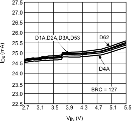
LM3535 30082419.gif
Figure 2. ILED vs Input Voltage 6 LEDs
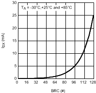
LM3535 30082423.gif
Figure 4. ILED vs Brightness Code Linear Scale
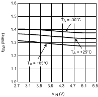
LM3535 30082431.gif
Figure 6. Switching Frequency vs Input Voltage Tri-Temp
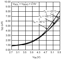
LM3535 30082428.gif
Figure 8. Shutdown Current vs Input Voltage VIO = 2.5 V
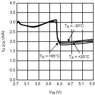
LM3535 30082430.gif
Figure 10. Quiescent Current vs Input Voltage 3/2× Gain
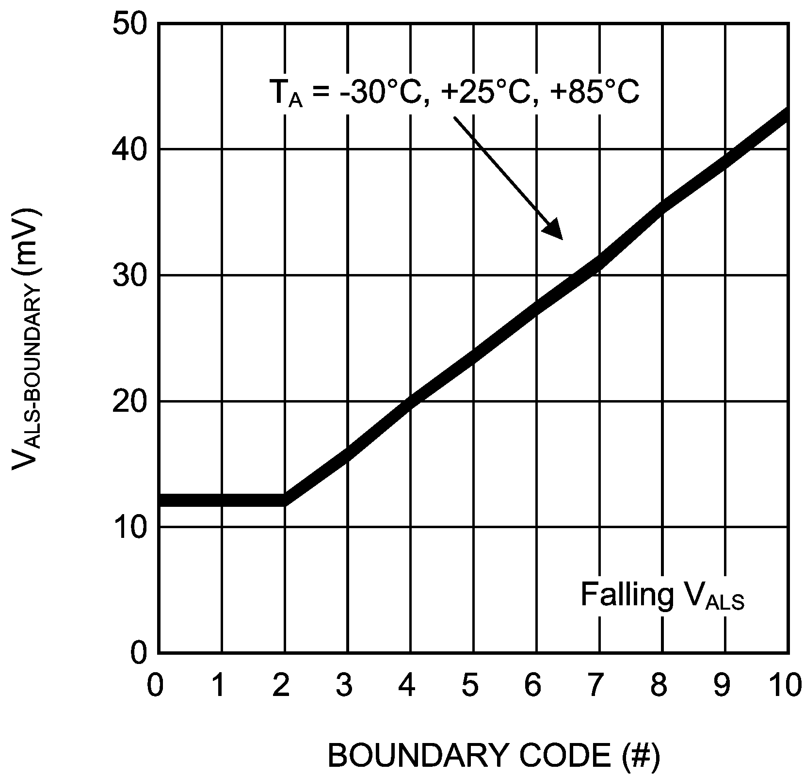
LM3535 30082471.png
Figure 12. ALS Boundary Voltage vs Boundary Code Falling ALS Voltage (Zoom)
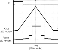
LM3535 30082454.gif
Figure 14. Ambient Light Sensor Response
LM3535 30082459.gif
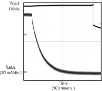
Figure 16. Diode Current Ramp-Down TSTEP = 6 ms
LM3535 30082420.gif
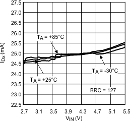
Figure 3. ILED vs Input Voltage
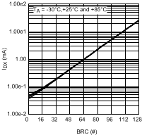
LM3535 30082422.gif
Figure 5. ILED vs Brightness Code Log Scale
LM3535 30082427.gif
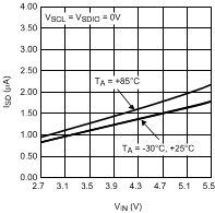
Figure 7. Shutdown Current vs Input Voltage VIO = 0 V
LM3535 30082429.gif
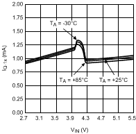
Figure 9. Quiescent Current vs Input Voltage 1× Gain
LM3535 30082470.png
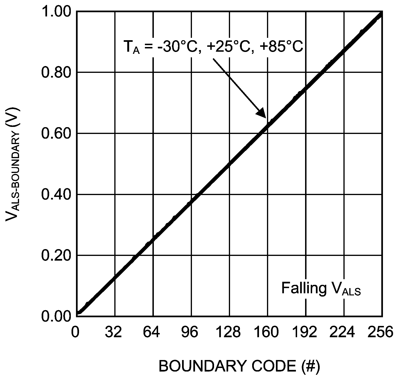
Figure 11. ALS Boundary Voltage vs Boundary Code Falling ALS Voltage
LM3535 30082453.gif
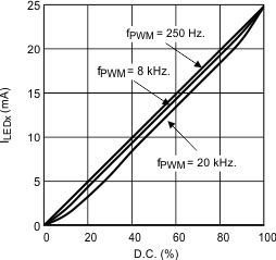
Figure 13. Diode Current vs PWM Duty Cycle
LM3535 30082458.gif
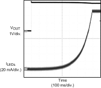
Figure 15. Diode Current Ramp-Up TSTEP = 6 ms