SNVS624B June 2011 – June 2016 LM3559
PRODUCTION DATA.
- 1 Features
- 2 Applications
- 3 Description
- 4 Revision History
- 5 Pin Configuration and Functions
- 6 Specifications
- 7 Typical Characteristics
-
8 Detailed Description
- 8.1 Overview
- 8.2 Functional Block Diagram
- 8.3
Feature Description
- 8.3.1 Power Amplifier Synchronization (TX1)
- 8.3.2 Input Voltage Flash Monitor Fault
- 8.3.3 Independent LED Control
- 8.3.4 Hardware Torch
- 8.3.5 Fault Protections
- 8.3.6 Input Voltage (VIN ) Monitor
- 8.3.7 VIN Flash Monitor (Flash Current Rising)
- 8.3.8 Last Flash Register
- 8.3.9 LED Voltage Monitor
- 8.3.10 ADC Delay
- 8.3.11 Flags Register and Fault Indicators
- 8.4
Device Functional Modes
- 8.4.1 Start-Up (Enabling the Device)
- 8.4.2 Pass Mode
- 8.4.3 Flash Mode
- 8.4.4 Torch Mode
- 8.4.5 Privacy-Indicate Mode
- 8.4.6 GPIO1 Mode
- 8.4.7 TX2/INT/GPIO2
- 8.4.8 TX2 Mode
- 8.4.9 GPIO2 Mode
- 8.4.10 Interrupt Output (INT Mode)
- 8.4.11 NTC Mode
- 8.4.12 Alternate External Torch (AET Mode)
- 8.4.13 Automatic Conversion Mode
- 8.4.14 Manual Conversion Mode
- 8.5 Programming
- 8.6
Register Maps
- 8.6.1 Enable Register
- 8.6.2 Torch Brightness Register
- 8.6.3 Flash Brightness Register
- 8.6.4 Flash Duration Register
- 8.6.5 Flags Register
- 8.6.6 Configuration Register 1
- 8.6.7 Configuration Register 2
- 8.6.8 GPIO Register
- 8.6.9 Last Flash Register
- 8.6.10 VLED Monitor Register
- 8.6.11 ADC Delay Register
- 8.6.12 Input Voltage Monitor Register
- 8.6.13 Privacy Register
- 8.6.14 Privacy PWM Period Register
- 8.6.15 Indicator Register
- 8.6.16 Indicator Blinking Register
- 9 Application and Implementation
- 10Power Supply Recommendations
- 11Layout
- 12Device and Documentation Support
- 13Mechanical, Packaging, and Orderable Information
Package Options
Mechanical Data (Package|Pins)
- YZR|16
Thermal pad, mechanical data (Package|Pins)
Orderable Information
9 Application and Implementation
NOTE
Information in the following applications sections is not part of the TI component specification, and TI does not warrant its accuracy or completeness. TI’s customers are responsible for determining suitability of components for their purposes. Customers should validate and test their design implementation to confirm system functionality.
9.1 Application Information
The LM3559 is a synchronous boost flash driver with dual 900-mA high-side current sources. The 2-MHz DC-DC boost regulator allows for the use of small external components. The device operates from a typical input voltage from 2.5 V to 5.5 V and an ambient temperature range of –40°C to +85°C.
Table 18. Application Circuit Component List
| COMPONENT | MANUFACTURER | VALUE | PART NUMBER | SIZE | RATING |
|---|---|---|---|---|---|
| L | Toko | 1 µH | FDSD0312-1R0 | 3 mm × 3 mm × 1.2 mm | 3.3 A |
| CIN/COUT | Murata | 10 µF | GRM188R60J106M | 1.6 mm × 0.8 mm × 0.8 mm (0603) | 6.3 V |
| LEDs | Lumiled | PWF-4 | VF = 3.6 V at 1 A |
9.2 Typical Applications
9.2.1 LM3559 Typical Application
 Figure 43. LM3559 Typical Application
9.2.1.1 Design Requirements
For typical LED flash driver applications, use the parameters listed in Table 19.
Table 19. Design Parameters
| DESIGN PARAMETER | EXAMPLE VALUE |
|---|---|
| Minimum input voltage | 2.5 V |
| Minimum output voltage | 1.8 V |
| Maximum output voltage | 5 V |
| Maximum output current | 1.8 A |
| Switching frequency | 2 MHz |
9.2.1.2 Detailed Design Procedure
9.2.1.2.1 Output Capacitor Selection
The LM3559 is designed to operate with at least a 10-µF ceramic output capacitor. When the boost converter is running the output capacitor supplies the load current during the boost converters on time. When the NMOS switch turns off the inductor energy is discharged through the internal PMOS switch, supplying power to the load and restoring charge to the output capacitor. This causes a sag in the output voltage during the on time and a rise in the output voltage during the off time. Therefore, choose the output capacitor to limit the output ripple to an acceptable level depending on load current and input/output voltage differentials and also to ensure the converter remains stable.
For proper operation the output capacitor must be at least a 10-µF ceramic. Larger capacitors such as a 22-µF or capacitors in parallel can be used if lower output voltage ripple is desired. To estimate the output voltage ripple considering the ripple due to capacitor discharge (ΔVQ) and the ripple due to the equivalent series resistance (ESR) of the capacitor (ΔVESR) use Equation 1 and Equation 2:
For continuous conduction mode, the output voltage ripple due to the capacitor discharge is:

The output voltage ripple due to the output capacitors ESR is found by:

In ceramic capacitors the ESR is very low so a close approximation is to assume that 80% of the output voltage ripple is due to capacitor discharge and 20% from ESR. Table 20 lists different manufacturers for various output capacitors and their case sizes suitable for use with the LM3559.
9.2.1.2.2 Input Capacitor Selection
Choosing the correct size and type of input capacitor helps minimize the voltage ripple caused by the switching of the device boost converter, and reduces noise on the input terminal of the boost converter that can feed through and disrupt internal analog signals. In the Figure 43 a 10-µF ceramic input capacitor works well. It is important to place the input capacitor as close as possible to the device input (IN) pin. This reduces the series resistance and inductance that can inject noise into the device due to the input switching currents. Table 20 lists various input capacitors that TI recommends for use with the LM3559.
Table 20. Recommended Input/Output Capacitors (X5r Dielectric)
| MANUFACTURER | PART NUMBER | VALUE | CASE SIZE | VOLTAGE RATING |
|---|---|---|---|---|
| TDK Corporation | C1608JB0J106M | 10 µF | 0603 (1.6 mm × 0.8 mm × 0.8 mm) | 6.3 V |
| TDK Corporation | C2012JB1A106M | 10 µF | 0805 (2 mm × 1.25 mm ×1.25 mm) | 10 V |
| TDK Corporation | C2012JB0J226M | 22 µF | 0805 (2 mm × 1.25 mm ×1.25 mm) | 6.3 V |
| Murata | GRM188R60J06M | 10 µF | 0603 (1.6 mm × 0.8 mm × 0.8 mm) | 6.3 V |
| Murata | GRM21BR61A106KE19 | 10 µF | 0805 (2 mm ×1.25 mm × 1.25 mm) | 10 V |
| Murata | GRM21BR60J226ME39L | 22 µF | 0805 (2 mm ×1.25 mm ×1.25 mm) | 6.3 V |
9.2.1.2.3 Inductor Selection
The LM3559 is designed to use a 1-µH or 2.2-µH inductor. Table 21 lists various inductors and their manufacturers that can work well with the LM3559. When the device is boosting (VOUT > VIN) the inductor typically is the largest area of efficiency loss in the circuit. Therefore, choosing an inductor with the lowest possible series resistance is important. Additionally, the saturation rating of the inductor must be greater than the maximum operating peak current of the LM3559. This prevents excess efficiency loss that can occur with inductors that operate in saturation and prevents overheating of the inductor and further efficiency loss. For proper inductor operation and circuit performance ensure that the inductor saturation and the peak current limit setting of the LM3559 is greater than IPEAK in Equation 3:

where
- ƒSW = 2 MHz
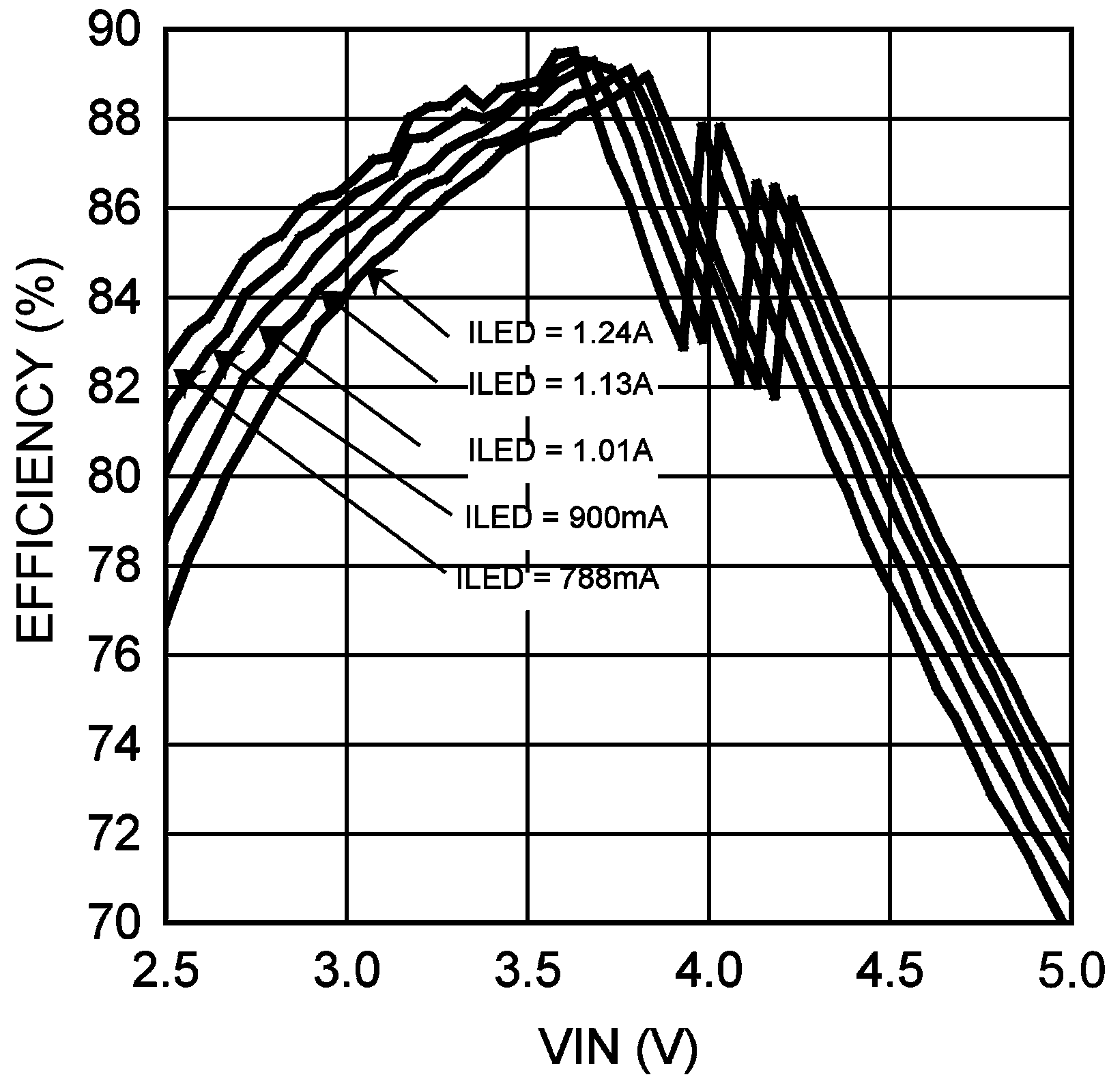
- Efficiency can be found in Typical Characteristics
Table 21. Recommended Inductors
| MANUFACTURER | L | PART NUMBER | DIMENSIONS (L×W×H) | ISAT | RDC |
|---|---|---|---|---|---|
| TOKO | 2.2 µH | FDSD0312-H-2R2M | 3 mm × 3.2 mm × 1.2 mm | 2.3 A | 105 mΩ |
| TOKO | 1 µH | FDSD0312-H-1R0M | 3 mm × 3.2 mm × 1.2 mm | 3.4 A | 43 mΩ |
| TOKO | 1.5 µH | FDSD0312-H-1R5M | 3 mm × 3.2 mm × 1.2 mm | 2.8 A | 71 mΩ |
| TOKO | 2.2 µH | FDSD0312-2R2M | 3 mm × 3.2 mm × 1.2 mm | 2.3 A | 145 mΩ |
| TOKO | 1 µH | FDSD0312-1R0M | 3 mm × 3.2 mm × 1.2 mm | 3.4 A | 70 mΩ |
| TDK | 1 µH | VLS4012ET-1R0N | 4 mm × 4 mm × 1.2 mm | 2.8 A | 50 mΩ |
| TDK | 2.2 µH | VLS252012T-2R2M1R3 | 2 mm × 2.5 mm × 1.2 mm | 1.5 A | 130 mΩ |
9.2.1.3 Application Curves

| Flash Brightness Codes 0xBB - 0xFF | ||

| Torch Brightness Codes 0x0F - 0xCF | ||

| Flash Brightness Codes 0x88 - 0xAA | ||

| Torch Brightness Codes 0x00 - 0x04 | ||
9.2.2 LM3559 Typical Application Circuit With Thermistor
 Figure 48. LM3559 Typical Application Circuit With Thermistor
9.2.2.1 Detailed Design Procedure
9.2.2.1.1 NTC Thermistor Selection
Programming bit [4] of Configuration Register 1 with a 1 selects NTC mode and makes the LEDI/NTC pin a comparator input for flash LED thermal sensing. Figure 48 shows the LM3559 using the NTC thermistor circuit. The thermal sensor resistor divider is composed of R3 and R(T), where R(T) is the Negative Temperature Coefficient Thermistor, VBIAS is the bias voltage for the resistive divider, and R3 is used to linearize the NTC's response around the NTC comparators trip point. CBYP is used to filter noise at the NTC input.
In designing the NTC circuit, we must choose values for VBIAS, R(T) and R3. To begin with, NTC thermistors have a non-linear relationship between temperature and resistance:

where β is given in the thermistor datasheet and R25C is the thermistors value at 25°C. R3 is chosen so that the temperature-to-resistance relationship becomes more linear and can be found by solving for R3 in the R(T) and R3 resistive divider:

where
- R(T)TRIP is the value of the thermistor at the temperature trip point
- VTRIP = 1 V (typical)
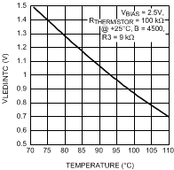
As an example, with VBIAS = 2.5 V and a thermistor whose nominal value at 25°C is 100 kΩ and a β = 4500 K, the trip point is chosen to be 93°C. The value of R(T) at 93°C is:

Figure 49 shows the linearity of the thermistor resistive divider of the previous example.
 Figure 49. Thermistor Resistive Divider Response vs Temperature