SNVS624B June 2011 – June 2016 LM3559
PRODUCTION DATA.
- 1 Features
- 2 Applications
- 3 Description
- 4 Revision History
- 5 Pin Configuration and Functions
- 6 Specifications
- 7 Typical Characteristics
-
8 Detailed Description
- 8.1 Overview
- 8.2 Functional Block Diagram
- 8.3
Feature Description
- 8.3.1 Power Amplifier Synchronization (TX1)
- 8.3.2 Input Voltage Flash Monitor Fault
- 8.3.3 Independent LED Control
- 8.3.4 Hardware Torch
- 8.3.5 Fault Protections
- 8.3.6 Input Voltage (VIN ) Monitor
- 8.3.7 VIN Flash Monitor (Flash Current Rising)
- 8.3.8 Last Flash Register
- 8.3.9 LED Voltage Monitor
- 8.3.10 ADC Delay
- 8.3.11 Flags Register and Fault Indicators
- 8.4
Device Functional Modes
- 8.4.1 Start-Up (Enabling the Device)
- 8.4.2 Pass Mode
- 8.4.3 Flash Mode
- 8.4.4 Torch Mode
- 8.4.5 Privacy-Indicate Mode
- 8.4.6 GPIO1 Mode
- 8.4.7 TX2/INT/GPIO2
- 8.4.8 TX2 Mode
- 8.4.9 GPIO2 Mode
- 8.4.10 Interrupt Output (INT Mode)
- 8.4.11 NTC Mode
- 8.4.12 Alternate External Torch (AET Mode)
- 8.4.13 Automatic Conversion Mode
- 8.4.14 Manual Conversion Mode
- 8.5 Programming
- 8.6
Register Maps
- 8.6.1 Enable Register
- 8.6.2 Torch Brightness Register
- 8.6.3 Flash Brightness Register
- 8.6.4 Flash Duration Register
- 8.6.5 Flags Register
- 8.6.6 Configuration Register 1
- 8.6.7 Configuration Register 2
- 8.6.8 GPIO Register
- 8.6.9 Last Flash Register
- 8.6.10 VLED Monitor Register
- 8.6.11 ADC Delay Register
- 8.6.12 Input Voltage Monitor Register
- 8.6.13 Privacy Register
- 8.6.14 Privacy PWM Period Register
- 8.6.15 Indicator Register
- 8.6.16 Indicator Blinking Register
- 9 Application and Implementation
- 10Power Supply Recommendations
- 11Layout
- 12Device and Documentation Support
- 13Mechanical, Packaging, and Orderable Information
Package Options
Mechanical Data (Package|Pins)
- YZR|16
Thermal pad, mechanical data (Package|Pins)
Orderable Information
8 Detailed Description
8.1 Overview
The LM3559 is a high-power white LED flash driver capable of delivering up to 1.8 A of LED current into a single LED, or up to 900 mA into two parallel LEDs. The device incorporates a 2-MHz constant frequency, synchronous boost converter, and two high-side current sources to regulate the LED current over the 2.5-V to 5.5-V input voltage range.
During operation when the output voltage is greater than VIN – 150 mV, the boost converter switches and maintains at least 270 mV across both current sources (LED1 and LED2). This minimum headroom voltage ensures that the current sinks remain in regulation. When the input voltage rises above the LED voltage + current source headroom voltage, the device stops switching and turns the PFET on continuously (pass mode). In pass mode the difference between (VIN - ILED × RON_P) and the voltage across the LEDs is dropped across the current sources.
Four hardware control pins provide control of the LM3559 device. These include a hardware flash enable (STROBE), dual flash-interrupt inputs (TX1 and TX2) designed to interrupt the flash pulse during high-battery current conditions, and a logic high hardware enable (HWEN) that can be pulled low to rapidly place the device into shutdown. Additional features of the LM3559 include an internal 4-bit ADC for LED voltage monitoring, an internal comparator for LED thermal sensing via an external NTC thermistor, a battery voltage monitor during flash current turnon which monitors VIN and optimizes the flash current during low-battery voltage conditions, an input voltage monitor that can force torch mode or LED shutdown of the flash current during input undervoltage conditions, a low-power Indicator current source with programmable patterns, and a mode for utilizing the flash LEDs as a privacy indicator.
Control of the LM3559 is done via an I2C-compatible interface. This includes adjustment of the flash and torch current levels, adjustment of the indicator LED currents and indicator pattern, changing the flash timeout duration, changing the switch current limit, and reading back the ADC results. Additionally, there are 8 flag bits that indicate flash current timeout, LED overtemperature, LED failure (by sensing LED short or output OVP condition during flash, torch, or privacy modes), device thermal shutdown, VIN undervoltage condition, tripping of the VIN flash monitor, and the occurrence of a TX interrupt (both TX1 and TX2).
8.2 Functional Block Diagram
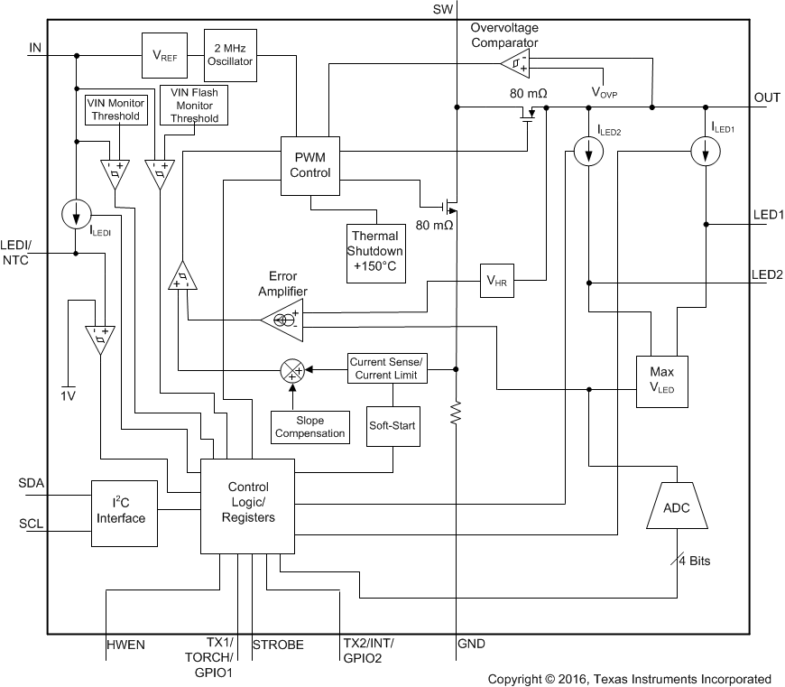
8.3 Feature Description
8.3.1 Power Amplifier Synchronization (TX1)
The TX1/TORCH/GPIO1 pin has a triple function. With the Configuration Register 1 Bit [7] = 0 (default) TX1/TORCH/GPIO1 is a power-amplifier-synchronization input. This mode is designed to reduce the flash LED current when TX1 is pulled high (active high polarity) or low (active low polarity). When the LM3559 is engaged in a flash event and the TX1/TORCH pin is pulled high, both LED1 and LED2 are forced into torch mode at the programmed torch current setting. If TX1 is then pulled low before the flash pulse terminates, the LED current returns to the previous flash current level. At the end of the flash timeout, whether the TX1/TORCH pin is high or low, the current sources turn off.
The polarity of the TX1 input can be changed from active high to active low by writing a 0 to bit [5] of Configuration Register 1. With this bit set to 0 the LM3559 is forced into torch mode when TX1/TORCH is pulled low. Figure 25 details the functionality of the TX1 interrupt.
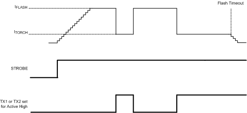 Figure 25. TX1 or TX2 Interrupt Event
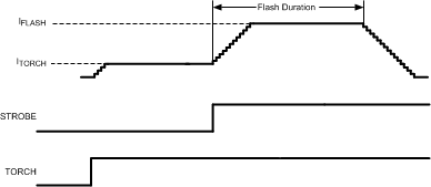 Figure 26. Hardware-Torch Mode
8.3.2 Input Voltage Flash Monitor Fault
The VIN flash monitor flag (bit [6] of the Flags Register reads back a 1 when the input voltage flash monitor is enabled and VIN falls below the programmed VIN flash monitor threshold. This flag must be read back in order to resume normal operation after the LED current has been forced to the lower flash current setting.
8.3.3 Independent LED Control
Bits [4:3] of the enable register provide for independent turnon and turnoff of the LED1 or LED2 current sources. The LED current is adjusted by writing to the Torch Brightness or Flash Brightness Registers. Both the Torch Brightness and the Flash Brightness Register provide for independent current programming for the LED currents in either LED1 or LED2. (See Torch Brightness Register and Flash Brightness Register descriptions.)
8.3.4 Hardware Torch
With Configuration Register 1 Bit [7] = 1, TX1/TORCH is configured as a hardware-torch-mode enable. In this mode (TORCH mode), a high at TX1/TORCH turns on the LED current at the programmed torch current setting. The STROBE input and I2C-enabled flash takes precedence over torch mode. In hardware-torch mode, both LED1 and LED2 current sources turn off after a flash event ,and Configuration Register 1 Bit [7] is reset to 0. In this situation, to re-enter torch mode via hardware torch, the hardware-torch enable bit (Configuration Register 1 Bit [7]) must be reset to 1. Figure 26 details the functionality of the TX1/TORCH/GPIO1 input.
8.3.5 Fault Protections
8.3.5.1 Overvoltage Protection
The output voltage is limited to typically 5 V (5.075 V maximum). In situations such as the current source open, the LM3559 raises the output voltage in order to keep the LED current at its target value. When VOUT reaches 5 V the overvoltage comparator trips and turns off both the internal NFET and PFET switches. When VOUT falls below 4.88 V (typical), the LM3559 begins switching again.
8.3.5.2 Current Limit
The LM3559 features 4 selectable current limits: 1.4 A, 2.1 A, 2.7 A, and 3.2 A. These are programmable through the I2C-compatible interface via bits [6:5] of the Flash Duration Register. When the current limit is reached, the LM3559 stops switching for the remainder of the switching cycle.
Since the current limit is sensed in the NMOS switch there is no mechanism to limit the current when the device operates in pass mode. In situations where there could potentially be large load currents at OUT and the LM3559 is operating in pass mode, the load current must be limited to 3 A. In boost mode or pass mode, if VOUT falls below approximately 2.3 V the part stops switching, and the PFET operates as a current source, limiting the current to typically 350 mA. This prevents damage to the LM3559 and prevents excessive current draw from the battery during output short-circuit conditions.
8.3.5.3 Flash Timeout
The flash-timeout period sets the amount of time that the flash current is being sourced from current sources LED1 and LED2. Bits [4:0] of the Flash Duration Register set the flash-timeout period. There are 32 different flash-timeout durations in steps of 32 ms giving a flash timeout range of 32 ms to 1024 ms (see Table 5).
8.3.5.4 Indicator LED/Thermistor (LEDI/NTC)
The LEDI/NTC pin serves a dual function, either as a programmable LED message indicator driver, or as a comparator input for negative temperature coefficient (NTC) thermistors.
8.3.5.4.1 Message Indicator Current Source (LEDI/NTC)
LEDI/NTC is configured as a message indicator current source by setting Configuration Register 1 bit [4] = 0. The indicator current source is enabled/disabled via Enable Register bit [6]. Enable Register bit [7] programs the message indictor for blinking mode. When the message indicator is set for blinking mode the pattern programmed into the Indicator Register and Indicator Blinking Register is sent to the message indicator current source.
The Indicator Blinking Register controls the following (see Table 17):
- Number of blank periods (BLANK#. This has 16 settings. tBLANK = tACTIVE × BLANK# , where tACTIVE = tPERIOD × PERIOD#
- Pulse width (tPULSE) has 16 settings between 0 and 480 ms in steps of 32 ms. The pulse width is the duration which the indicator current is at its programmed set point at the end of the ramp-up time.
The Indicator Register controls the following (see Table 16):
- Indicator current level (IIND). There are 8 message indicator current levels from 2.25 mA to 18 mA in steps of 2.25 mA.
- Number of periods (PERIOD#). This has 8 steps. A period (tPERIOD) is found by (tPERIOD = tR + tF + 2 × tPULSE). (See Figure 27 for indicator timing).
- Ramp times (tR or tF) for turnon and turnoff of the indicator current source. Four programmable times of 78 ms, 156 ms, 312 ms, and 624 ms are available. The ramp times apply for both ramp-up and ramp-down and are not independently changeable.
 Figure 27. Message Indicator Timing Diagram
8.3.5.4.1.1 Message Indicator Example 1 (Single Pulse With Dead Time):
As an example, to set up the message indicator for a 312-ms ramp-up and ramp-down, 192 ms pulse width, and 1 pulse followed by a 5-s delay. The indicator settings will be as follows. tR = tF = 312 ms, tWIDTH = 192 ms (tPERIOD = 312 ms × 2 + 192 ms × 2 = 1016 ms). BLANK# setting will be: 5 s / 1016 ms × 1 (PERIOD# = 1). Giving a BLANK# setting of 5. The resulting waveform appears as shown in Figure 28.
 Figure 28. Message Indicator Example 1
8.3.5.4.1.2 Message Indicator Example 2 (Multiple Pulses With Dead Time):
Another example has the same tR, tF, tPULSE, and tBLANK times as before, but this time the PERIOD# is set to 3. Now the tACTIVE time is tPERIOD × 3 = 1016 ms × 3 = 3048 ms. This results in a blank time of tBLANK = tACTIVE × BLANK# = 3.048 s × 5 = 15.24 s (see Figure 29).
 Figure 29. Message Indicator Example 2
8.3.5.4.1.3 Updating The Message Indicator
The best way to update the message indicator is to disable the message indicator output via the Enable Register bit [7], write the new sequence to the Indicator Register and/or Indicator Blinking Register, and then re-enable the message indicator. Updating the Indicator Registers on the fly can lead to long delays between pattern changes. This is especially true if the PERIOD# or BLANK# setting is changed from a high setting to a lower setting.
8.3.6 Input Voltage (VIN ) Monitor
The LM3559 has an internal comparator at IN that monitors the input voltage and can force the LED current into torch mode or into shutdown, if VIN falls below the programmable VIN monitor threshold. Bit 0 in the VIN Monitor Register enables or disables this feature. Bits [2:1] of the VIN Monitor Register program the 4 adjustable thresholds of 2.9 V, 3 V, 3.1 V, and 3.2 V. Bit 3 in Configuration Register 2 selects whether an undervoltage event forces torch mode or forces the LEDs off. See Table 13 for additional information. When the VIN monitor is active and VIN falls below the programmed VIN Monitor threshold, the active current sources (LED1 and/or LED2) either turns off or is forced into the torch current setting. To reset the LED current to its previous level, VIN must go above the VIN monitor threshold and the Flags Register must be read back. See Figure 30 for the VIN monitor timing waveform.
To avoid noise from falsely triggering the VIN monitor, this mode incorporates a 250 µs deglitch timer. With the VIN monitor active, VIN must go below the VIN monitor threshold (VIN_TH) and remain below it for 250 µs before the LEDs are forced into torch mode (or shut down) and the VIN monitor flag is written.
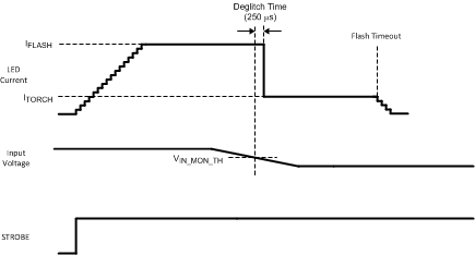 Figure 30. VIN Monitor Waveform
8.3.7 VIN Flash Monitor (Flash Current Rising)
A second comparator at IN is available to monitor the input voltage during the flash current turnon. Bit [3] of the VIN Monitor Register enables/disables this feature. With this bit set to 1 the VIN flash monitor is active. Bits [5:4] of the VIN Monitor Register program the 4 selectable thresholds of (2.9 V, 3 V, 3.1 V, and 3.2 V). The feature operates as follows: during flash current turnon the active current sources (LED1 and/or LED2) transition through each of the lower flash and torch current levels until the target flash current is reached. With the VIN flash monitor active, if the input voltage falls below the VIN flash monitor threshold during the flash current turnon,the flash current is set to the level that the current ramp had risen to at the time of the undervoltage event. The VIN flash monitor only operates during the ramping up of the flash LED current.
The VIN flash monitor ignores the first 2 flash codes during the flash pulse turnon. As a result, if the VIN flash monitor is enabled, and VIN were to fall below the VIN flash threshold as the LED current ramps up through either of the first two levels, then the flash pulse would not be halted until code #3 (168.75-mA per current source).
To avoid noise from falsely triggering the VIN flash monitor, this mode incorporates an 8-µs deglitch timer as well as an internal analog filter at the input of the VIN flash monitor comparator. With the VIN flash monitor active, VIN must go below the VIN flash monitor threshold (VIN_FLASH) and remain below it for 8 µs before the flash current ramp is halted and the VIN flash monitor flag is written.
8.3.8 Last Flash Register
Once the VIN flash monitor is tripped, the flash code that corresponded to the LED current at which the flash current ramp was halted is written to the Last Flash Register. The Last Flash Register is a read-only register; the lower 4 bits are available to latch the code for LED1 and the upper 4 bits to latch the code for LED2.
For example, suppose that the LM3559 device is set up for a single LED with a target flash current of 1125 mA. The VIN flash monitor is enabled with the VIN flash monitor threshold set to 3. V (VIN Monitor Register bits [5:4] = 0, 1). When the STROBE input is brought high, the LED current begins ramping up through the torch and flash codes at 32 µs per code. As the input current increases, the input voltage at the device IN pin begins to fall due to the source impedance of the battery. By the time the LED current has reached 900 mA (code 0x77 or 450 mA per current source), VIN falls below 3 V. The VIN flash monitor then stops the flash current ramp and the device continues to proceed with the flash pulse, but at 900 mA instead of 1125 mA. Figure 31 details this sequence.
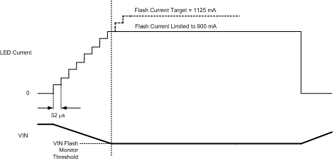 Figure 31. VIN Flash Monitor Example
8.3.9 LED Voltage Monitor
The LM3559 includes a 4-bit ADC which monitors the LED forward voltage (VLED) and stores the digitized value in bits [3:0] of the VLED Monitor Register. The highest voltage of VLED1 or VLED2 is automatically sensed and that becomes the sample point for the ADC. Bit 5, the ADC shutdown bit, enables or disables the ADC with the default state set to enable (bit [5] = 0).
8.3.10 ADC Delay
The ADC Delay Register provides for a programmable delay from 250 µs to 8 ms, in steps of 250 µs. This delay is the delay from when the EOC bit goes low to when the VLED monitor samples the LED voltage. In automatic mode the EOC bit goes low when the Flash LED current hits its target. In manual mode the EOC bit goes low at the end of a readback of the VLED Monitor Register (or when the manual mode bit (bit 4) is re-written with a 1). Figure 32 and Figure 33 detail the timing of the VLED Monitor for both automatic mode and manual mode.
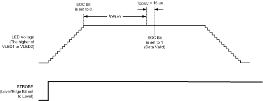 Figure 32. VLED Monitor Automatic Mode
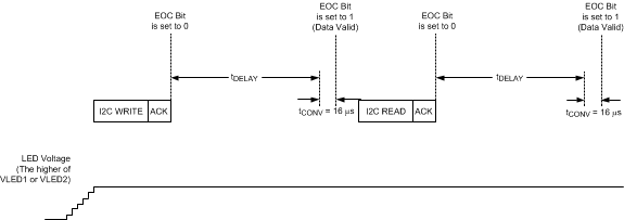 Figure 33. VLED Monitor Manual Mode
8.3.11 Flags Register and Fault Indicators
Eight fault flags are available in the LM3559. These include: a flash timeout, a thermal shutdown, an LED failure flag (LEDF), an LED thermal flag (NTC), a VIN monitor flag, and a VIN flash monitor flag. Additionally, two LED interrupt flag bits (TX1 interrupt and TX2 interrupt) are set when the corresponding interrupt is activated. Reading back a 1 indicates the flagged event has happened. A read of the Flags Register resets these bits.
8.3.11.1 Flash Timeout
The timeout (or TO flag, (bit [0] of the Flags Register), reads back a 1 if the LM3559 is active in flash mode and the timeout period expires before the flash pulse is terminated. The flash pulse can be terminated before the timeout period expires by pulling the STROBE pin low (with Enable Register bit [5] = 0), or by writing a (0,0) to bits [1:0] of the Enable Register. The TO flag is reset to 0 by pulling HWEN low, removing power to the LM3559 device, reading the Flags Register, or when the next flash pulse is triggered.
8.3.11.2 Thermal Shutdown
When the die temperature of the LM3559 device reaches 150°C, the boost converter shuts down, and the NFET and PFET turn off. Additionally, the active current source (LED1 and/or LED2) turn off. When the thermal shutdown threshold is tripped a 1 is written to bit [1] of the Flags Register (thermal shutdown bit). The device does not start up again until the die temperature falls to below 135°C and the Flags Register is read back, or when the device is shut down and started up again.
8.3.11.3 LED Fault
The LED Fault flag (bit 2 of the Flags Register) reads back a 1 if the part is active in either flash or torch mode and either LED1 or LED2 experience an open or short condition. An LED open condition is signaled if the OVP threshold is crossed at the OUT pin while the device is in either flash or torch mode. An LED short condition is signaled if the voltage at LED1 or LED2 goes below 500 mV while the device is in torch or flash mode. In an LED open condition there is a 2-µs deglitch time from when the output voltage crosses the OVP threshold to when the LED fault flag is triggered. In an LED short condition there is a 250-µs deglitch time before the LED fault flag is set. The LED fault flag can only be reset to 0 by pulling HWEN low, doing a power-on reset of the LM3559, or by removing the fault condition and reading back the Flags Register.
8.3.11.4 TX1 and TX2 Interrupt Flags
The TX1 and TX2 interrupt flags (bits [3] and [4]) indicate an interrupt event has occurred on the respective TX inputs. Bit 3 reads back a 1 if TX1 is in TX mode and there has been a TX1 event since the last read of the Flags Register. Bit 4 read back a 1 if TX2 is in TX mode and there has been a TX2 event since the last read of the Flags Register. A read of the Flags Register automatically resets these bits. A TX event on TX1 or TX2 can be a high-to-low transition or a low-to-high transition depending on the setting of the TX1 and TX2 polarity bits (see Configuration Register 1 Bits [6:5]).
8.3.11.5 LED Thermal Fault (NTC Flag)
The NTC flag (bit [5] of the Flags Register) reads back a 1 if the LM3559 is active in flash or torch mode, the device is in NTC mode, and the voltage at LEDI/NTC has fallen below VTRIP (1 V typical). When this has happened and the LM3559 has been forced into torch mode or LED shutdown (depending on the state of Configuration Register 2 bit [1), the Flags Register must be read, and the voltage at NTC must go above 1 V in order to place the device back in normal operation. (See NTC Mode for more details.)
8.3.11.6 Input Voltage Monitor Fault
The VIN monitor flag (bit [7] of the Flags Register) reads back a 1 when the Input Voltage Monitor is enabled and VIN falls below the programmed VIN monitor threshold. This flag must be read back and VIN must go above the VIN monitor threshold in order to resume normal operation.
8.4 Device Functional Modes
8.4.1 Start-Up (Enabling the Device)
Turnon of the LM3559 is done through bits [1:0] of the Enable Register. Bits [1:0] enable the device in torch mode, flash mode, or privacy Indicate mode. Additionally, bit 6 enables the message indicator at the LEDI/NTC pin. On start-up, when VOUT is less than VIN, the internal synchronous PFET turns on as a current source and delivers 350 mA to the output capacitor. During this time both current sources (LED1, and LED2) are off. When the voltage across the output capacitor reaches 2.2 V the active current sources can turn on. At turnon the current sources step through each flash and torch level until their target LED current is reached (32 µs/step). This gives the device a controlled turnon and limits inrush current from the VIN supply.
8.4.2 Pass Mode
At turnon, when the output voltage charges up to (VIN – 150 mV), the device operates in either pass mode or boost mode, depending upon the voltage difference between VOUT and VLED. If the voltage difference between VOUT and VLED is less than 270 mV, the device operates in boost mode. If the difference between VOUT and VLED is greater than 270 mV, the device operates in pass mode. In pass mode the boost converter stops switching, and the synchronous PFET turns fully on, bringing VOUT up to VIN – IIN × RPMOS (RPMOS = 80 mΩ). In pass mode the inductor current is not limited by the peak current limit. In this situation the output current must be limited to 3 A.
8.4.3 Flash Mode
In flash mode the LED current sources (LED1 and LED2) each provide 16 different current levels from typically 56.25 mA (total) to 1.8 A (total) in steps of 56.25 mA. The flash currents are adjusted via the Flash Brightness Register. Flash mode is activated by writing a 1, 1 to bits [1:0] of the Enable Register or by enabling the hardware flash input (STROBE) via bit [2] of Configuration Register 1 and then pulling the STROBE pin high (high polarity). Once the flash sequence is activated both current sinks (LED1 and LED2) ramp up to their programmed flash current level by stepping through all torch and flash levels (32 µs/step) until the programmed current is reached.
Bit [5] of the Enable Register (STROBE Level/Edge bit) determines how the flash pulse terminates. With the Level/Edge bit = 1 the flash current only terminates when it reaches the end of the flash timeout period. With the level/edge bit = 0, flash mode can be terminated by pulling STROBE low, programming bits [1:0] of the Enable Register with 0,0, or by allowing the flash timeout period to elapse. If the level/edge bit = 0 and STROBE is toggled before the end of the flash timeout period the timeout period resets. Figure 34 and Figure 35 detail the flash pulse termination for the different level/edge bit settings.
![LM3559 LED Current for Strobe (Level
Triggered, Enable Register Bit [5] = 0)
Strobe Goes Low Before the End of the Programmed Timeout Duration LM3559 30102803.gif](/ods/images/SNVS624B/30102803.gif) Figure 34. LED Current for Strobe (Level Triggered, Enable Register Bit [5] = 0)
Figure 34. LED Current for Strobe (Level Triggered, Enable Register Bit [5] = 0)Strobe Goes Low Before the End of the Programmed Timeout Duration
![LM3559 LED Current for Strobe (Edge
Triggered, Enable Register Bit [5] = 1) LM3559 30102804.gif](/ods/images/SNVS624B/30102804.gif) Figure 35. LED Current for Strobe (Edge Triggered, Enable Register Bit [5] = 1)
Figure 35. LED Current for Strobe (Edge Triggered, Enable Register Bit [5] = 1)
After the flash pulse terminates; either by a flash timeout, pulling STROBE low or disabling it via the I2C-compatible interface, LED1 and LED2 turn completely off. This happens even when torch is enabled via the I2C-compatible interface, and the flash pulse is turned on by toggling STROBE. After a flash event ends, the EN1, EN0 bits (bits [1:0] of the Enable Register) are automatically reset with 0, 0. The exception occurs when the privacy terminate bit is low (bit [3]) in the Privacy Register. In this case, the specific current source that is enabled for privacy mode turns back on after the flash pulse if privacy mode had been enabled before the flash pulse.
8.4.4 Torch Mode
In torch mode the current sources LED1 and LED2 each provide 8 different current levels (Table 3). Torch mode is activated by setting Enable Register bits [1:0] to (1, 0). Once torch mode is enabled, the current sources ramp up to the programmed torch current level by stepping through all of the torch currents at (32 µs/step) until the programmed torch current level is reached.
8.4.5 Privacy-Indicate Mode
The current sources (LED1 and/or LED2) can also be used as a privacy indicator before and after flash mode. Privacy-indicate mode is enabled by setting the Enable Register bit [1:0] to (0,1). Additionally, the Privacy Register contains the bits to select which current source to use as the privacy indicator (either LED1, LED2, or both), whether or not the privacy-indicate mode turns off at the end of the flash pulse, and contains the 8 intensity levels for the privacy indicator.
The intensity of the LEDs in privacy indicate mode is set by PWM’ing the lowest torch current level (28.125 mA). Bits [2:0] of the Privacy Register allow for 8 different duty cycles of 10%, 20%, 30%, 40%, 50%, 60%, 70%, and 80%. See Table 14 for Privacy Register bit settings. Figure 36 details the timing for the privacy-indicate mode on ILED1 or ILED2.
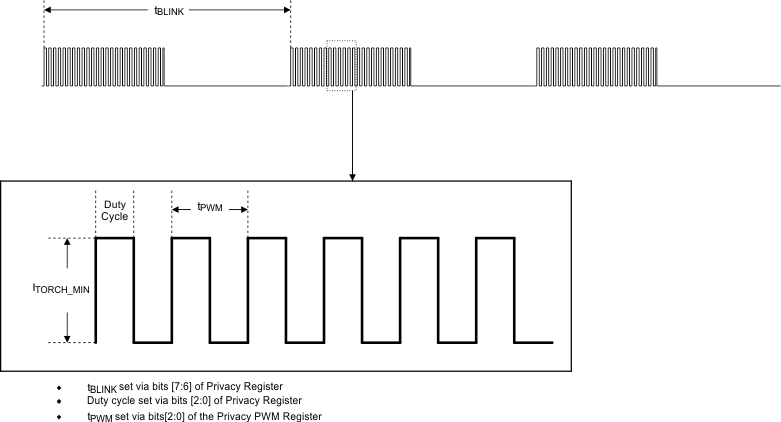 Figure 36. Privacy Indicate Timing
8.4.6 GPIO1 Mode
With bit [0] of the GPIO Register set to 1, the TX1/TORCH/GPIO1 pin is configured as a logic I/O. In this mode the TX1/TORCH/GPIO1 pin is readable and writable as a logic input/output via bits [2:1] of the GPIO Register. See Table 9.
8.4.7 TX2/INT/GPIO2
The TX2/INT/GPIO2 pin has a triple function. In TX2 mode (default) the TX2/INT/GPIO2 pin is an active high flash interrupt. With GPIO Register bit [3] = 1 the TX2/INT/GPIO2 pin is configured as general purpose logic I/O. With GPIO Register bit [6] = 1, and with the TX2/INT/GPIO2 pin configured as a GPIO2 output, the TX2/INT/GPIO2 pin is an interrupt output.
8.4.8 TX2 Mode
In TX2 mode, when Configuration Register 1, bit [6] = 0, the TX2/INT/GPIO2 pin has active low polarity. Under this condition when the LM3559 is engaged in a flash event and TX2 is pulled low, both LED1 and LED2 are forced into torch mode. In TX2 mode with Configuration Register 1, bit [6] = 1 the TX2/INT/GPIO2 input has active high polarity. Under this condition when the LM3559 is engaged in a flash event and the TX2/INT/GPIO2 pin is driven high, both LED1 and LED2 are forced into torch mode. During a flash interrupt event if the TX2/INT/GPIO2 input is disengaged the LED current returns to the previous flash current level. During a flash event, if TX2 is active, the LED current sources still turn off after the flash timeout. Figure 25 details the functionality of the TX2 Interrupt.
8.4.8.1 TX2 Shutdown
TX2 also has the capability to force shutdown. Bit [0] of Configuration Register 2 set to a 1 changes the TX2 mode from a force torch when active to a force shutdown when active. For example, if TX2/INT/GPIO2 is configured for TX2 mode with active high polarity, and bit [0] of Configuration Register 2 is set to 1 then when TX2 is driven high, the active current sources (LED1 and/or LED2) are forced into shutdown. Once the active current sources are forced into shutdown by activating TX2, the current sources can only be re-enabled if TX2 is deactivated, and the Flags Register is read back.
8.4.9 GPIO2 Mode
With Bit [3] of the GPIO Register set to 1, the TX2/INT/GPIO2 pin is configured as a logic I/O. In this mode the TX2/INT/GPIO2 pin is readable and writeable as a logic input/output via bits [5:4] of the GPIO Register. See Table 9.
8.4.10 Interrupt Output (INT Mode)
The TX2/INT/GPIO2 pin can be reconfigured as an active low interrupt output by setting bit [6] in the GPIO Register to 1 and configuring TX2/INT/GPIO2 as a GPIO2 output. In this mode, TX2/INT/GPIO2 pulls low when any of these conditions exist.
- The LM3559 is configured for NTC mode (Configuration Register 1 bit [4] = 1) and the voltage at LEDI/NTC has fallen below VTRIP (1 V typical).
- The LM3559 is configured for VIN monitor mode (VIN Monitor Register bit [0] = 1) and VIN is below the programmed VIN Monitor Threshold.
- The LM3559 is configured for VIN flash monitor mode (VIN Monitor Register bit [3] = 1) and VIN falls below the programmed VIN flash monitor threshold. Figure 37 shows the functionality of the TX2/INT/GPIO2 input.
Once INT is pulled low due to any of the above conditions having been met, INT only goes back high again if any of the conditions are no longer true and the Flags Register is read.
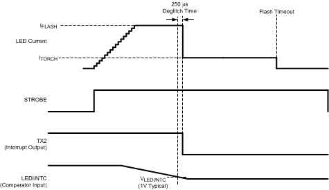 Figure 37. TX2 as an Interrupt Output (During an NTC Event)
8.4.11 NTC Mode
Writing a 1 to the Configuration Register 1 bit [4] configures the LEDI/NTC pin for NTC mode. In this mode the indicator current source is disabled and LEDI/NTC becomes the positive input to the NTC comparator. NTC mode operates as a LED current interrupt that is triggered when the voltage at LEDI/NTC goes below 1 V.
Two actions can be taken when the NTC comparator is tripped. With Configuration Register 2 bit [1] set to 0 the NTC interrupt forces the LED current from flash mode into torch mode. With Configuration Register 2 bit [1] set to 1 the NTC interrupt forces the LED current into shutdown.
Whether in NTC force torch or NTC shutdown, in order to re-enter flash mode or torch mode after an NTC event, two things must occur. First, the NTC input must be above the 1-V threshold. Secondly, the Flags Register must be read.
To avoid noise from falsely triggering the NTC comparator, this mode incorporates a 250-µs deglitch timer. With NTC mode active, VLEDI/NTC must go below the trip point (VTRIP), and remain below it, for 250 µs before the LEDs are forced into torch mode (or shut down) and the NTC flag is written.
8.4.12 Alternate External Torch (AET Mode)
Configuration Register 2 bit [2] programs the LM3559 for AET mode. With this bit set to 0 (default) TX1/TORCH is a flash current interrupt that forces torch mode only during a flash event. For example, if TX1/TORCH goes high while the LED current is in flash mode, the LEDs are forced into torch mode only for the duration of the timeout counter. At the end of the timeout counter the LEDs turn off.
With the Configuration Register 2 bit [2] set to 1 the LM3559 is configured for AET mode and the operation of TX1/TORCH becomes dependent on its occurrence relative to the STROBE input. In this mode, if TX1/TORCH goes high first, then STROBE goes high next, the LEDs are forced into Torch mode with no timeout. In this mode, if TX1/TORCH goes high after STROBE has gone high, then the TX1/TORCH pin operates as a normal LED current interrupt and the LEDs turn off at the end of the timeout duration (see Figure 38.
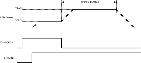 Figure 38. AET Mode Timing
8.4.13 Automatic Conversion Mode
With the ADC enabled, a conversion is performed each time a flash pulse is started. When a flash pulse is started bit [6] of the VLED Monitor Register (end-of-conversion bit) is automatically written with a 0. At the end of the conversion, bit [6] goes high signaling that the VLED data is valid. A read back of the VLED Monitor Register clears the EOC bit. Figure 32 shows the VLED monitor automatic conversion.
8.4.14 Manual Conversion Mode
The VLED monitor can be set up for manual conversion mode by setting bit [4] of the VLED Monitor Register to 1. When this bit is set high the EOC bit (bit [6]) goes low, and a conversion is performed. When the conversion is complete, the EOC bit goes high again. Subsequent conversions are performed in manual mode by reading back the VLED Monitor Register, which resets the EOC bit and starts another conversion (see Figure 33).
8.5 Programming
8.5.1 I2C-Compatible Interface
8.5.1.1 START and STOP Conditions
The LM3559 is controlled via an I2C-compatible interface. START and STOP conditions classify the beginning and end of the I2C session. A START condition is defined as SDA transitioning from HIGH to LOW while SCL is HIGH. A STOP condition is defined as SDA transitioning from LOW to HIGH while SCL is HIGH. The I2C master always generates the START and STOP conditions.
 Figure 39. START and STOP Sequences
The I2C bus is considered busy after a START condition and free after a STOP condition. During data transmission the I2C master can generate repeated START conditions. A START and a repeated START condition are equivalent function-wise. The data on SDA must be stable during the HIGH period of the clock signal (SCL). In other words, the state of SDA can only be changed when SCL is LOW. Figure 40 shows the SDA and SCL signal timing for the I2C-Compatible bus. See the Electrical Characteristics for timing values.
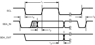 Figure 40. I2C-Compatible Timing
8.5.1.2 I2C-Compatible Chip Address
The device address for the LM3559 is 1010011 (0xA7 for read and 0xA6 for write). After the START condition, the I2C master sends the 7-bit address followed by an eighth read or write bit (R/W). R/W = 0 indicates a WRITE and R/W = 1 indicates a READ. The second byte following the device address selects the register address to which the data will be written. The third byte contains the data for the selected register.
 Figure 41. Device Address
8.5.1.3 Transferring Data
Every byte on the SDA line must be eight bits long, with the most significant bit (MSB) transferred first. Each byte of data must be followed by an acknowledge bit (ACK). The acknowledge related clock pulse (9th clock pulse) is generated by the master. The master releases SDA (HIGH) during the 9th clock pulse (write mode). The LM3559 pulls down SDA during the 9th clock pulse, signifying an acknowledge. An acknowledge is generated after each byte has been received.
8.6 Register Maps
Table 1. LM3559 Internal Registers
| REGISTER NAME | INTERNAL HEX ADDRESS | POWER-ON/RESET VALUE |
|---|---|---|
| Enable | 0x10 | 0x18 |
| Privacy | 0x11 | 0x58 |
| Indicator | 0x12 | 0x00 |
| Indicator Blinking | 0x13 | 0x00 |
| Privacy PWM | 0x14 | 0xF0 |
| GPIO | 0x20 | 0x80 |
| VLED Monitor (ADC) | 0x30 | 0x80 |
| ADC Delay | 0x31 | 0xC0 |
| VIN Monitor | 0x80 | 0xC0 |
| Last Flash | 0x81 | 0x00 |
| Torch Brightness | 0xA0 | 0x52 |
| Flash Brightness | 0xB0 | 0xDD |
| Flash Duration | 0xC0 | 0x6F |
| Flags | 0xD0 | 0x00 |
| Configuration 1 | 0xE0 | 0x68 |
| Configuration 2 | 0xF0 | 0xF0 |
8.6.1 Enable Register
Bits [1:0] of the Enable Register controls the ON/OFF state of torch mode, flash mode, and privacy-indicate mode. Bits [4:3] turn on/off the main current sources (LED1 and LED2). Bit [5] sets the level or edge control for the STROBE input. Bits 7 and 6 control the indicator current source (see Table 2).
Table 2. Enable Register Descriptions
| Bit 7 (EN Blink) |
Bit 6 (EN Message Indicator) |
Bit 5 (STROBE Level/Edge) |
Bit 4 (LED2 Enable) |
Bit 3 (LED1 Enable) |
Bit 2 (Not Used) |
Bit 1 (EN1) |
Bit 0 (EN0) |
|---|---|---|---|---|---|---|---|
| 0 = Message indicator blinking function is disabled(1) (default)
1 = message indicator blinking function is enabled. The message indicator blinks the pattern programmed in the Indicator Register and Indicator Blinking Register |
0 = Message Indicator is disabled (default)
1= Message Indicator is enabled. |
0 = (Level Sensitive) When STROBE goes high, the flash current will turn on and remain on for the duration the STROBE pin is held high or until the flash timeout occurs, whichever comes first. (default) 1 = (Edge Triggered) When STROBE goes high , the flash current will turn on and remain on for the duration of the Flash timeout. |
0 = LED2 off 1 = LED2 on (default) |
0 = LED1 off 1 = LED1 on (default) |
N/A | Enable Bits
00 = Current sources are shut down (default) 01 = Privacy-indicate mode 10 = Torch mode 11 = Flash mode (bits reset at timeout) |
|
8.6.2 Torch Brightness Register
Bits [2:0] of the Torch Brightness Register set the Torch current for LED1. Bits [5:3] set the torch current for LED2. (see Table 3).
Table 3. Torch Brightness Register Descriptions
| Bit 7 (N/A) |
Bit 6 (N/A) |
Bit 5 (TC2A) |
Bit 4 (TC2B) |
Bit 3 (TC2C) |
Bit 2 (TC1A) |
Bit 1 (TC1B) |
Bit 0 (TC1C) |
|---|---|---|---|---|---|---|---|
| (Not Used) | LED2 Torch Current Select Bits
000 = 28.125 mA (56.25 mA total) 001 = 56.25 mA (112.5 mA total) 010 = 84.375 mA (168.75 mA total) default 011 = 112.5 mA (225 mA total) 100 = 140.625 mA (281.25 mA total) 101 = 168.75 mA (337.5 mA total) 110 = 196.875 mA (393.75 mA total) 111 = 225 mA (450 mA total) |
LED1 Torch Current Select Bits
000 = 28.125 mA (56.25 mA total) 001 = 56.25 mA (112.5 mA total) 010 = 84.375 mA (168.75 mA total) default 011 = 112.5 mA (225 mA total) 100 = 140.625 mA (281.25 mA total) 101 = 168.75 mA (337.5 mA total) 110 = 196.875 mA (393.75 mA total) 111 = 225 mA (450 mA total) |
|||||
8.6.3 Flash Brightness Register
Bits [3:0] of the Flash Brightness Register set the Flash current for LED1. Bits [7:4] set the Flash current for LED2. (see Table 4).
Table 4. Flash Brightness Register Descriptions
| Bit 7 (FC2A) |
Bit 6 (FC2B) |
Bit 5 (FC2C ) |
Bit 4 (FC2D) |
Bit 3 (FC1A ) |
Bit 2 (FC1B) |
Bit 1 (FC1C) |
Bit 0 (FC1D) |
|---|---|---|---|---|---|---|---|
| LED2 Flash Current Select Bits
0000 = 56.25 mA (112.5 mA total) 0001 = 112.5 mA (225 mA total) 0010 = 168.75 mA (337.5 mA total) 0011 = 225 mA (450 mA total) 0100 = 281.25 mA (562.5 mA total) 0101 = 337.5 mA (675 mA total) 0110 = 393.75 mA (787.5 mA total) 0111 = 450 mA (900 mA total) 1000 = 506.25 mA (1012.5 mA total) 1001 = 562.5 mA (1125 mA total) 1010 = 618.75 mA (1237.5 mA total) 1011 = 675 mA (1350 mA total) 1100 = 731.25 mA (1562.5 mA total) 1101 = 787.5 mA (1575 mA total) Default 1110 = 843.75 mA (1687.5 mA total) 1111 = 900 mA (1800 mA total) |
LED1 Flash Current Select Bits
0000 = 56.25 mA (112.5 mA total) 0001 = 112.5 mA (225 mA total) 0010 = 168.75 mA (337.5 mA total) 0011 = 225 mA (450 mA total) 0100 = 281.25 mA (562.5 mA total) 0101 = 337.5 mA (675 mA total) 0110 = 393.75 mA (787.5 mA total) 0111 = 450 mA (900 mA total) 1000 = 506.25 mA (1012.5 mA total) 1001 = 562.5 mA (1125 mA total) 1010 = 618.75 mA (1237.5 mA total) 1011 = 675 mA (1350 mA total) 1100 = 731.25 mA (1562.5 mA total) 1101 = 787.5 mA (1575 mA total) Default 1110 = 843.75 mA (1687.5 mA total) 1111 = 900 mA (1800 mA total) |
||||||
8.6.4 Flash Duration Register
Bits [4:0] of the Flash Duration Register set the flash timeout duration. Bits [6:5] set the switch current limit (see Table 5).
Table 5. Flash Duration Register Descriptions
| Bit 7 (Not used) |
Bit 6 (CL1) |
Bit 5 (CL0) |
Bit 4 (T4) |
Bit 3 (T3) |
Bit 2 (T2) |
Bit 1 (T1) |
Bit 0 (T0) |
|---|---|---|---|---|---|---|---|
| N/A | Current Limit Select Bits
00 = 1.4 A peak current limit 01 = 2.1 A peak current limit 10 = 2.7 A peak current limit 11 = 3.2 A peak current limit (default) |
Flash timeout Select Bits
00000 = 32 ms timeout 00001 = 64 ms timeout 00010 = 96 ms timeout 00011 = 128 ms timeout 00100 = 160 ms timeout 00101 = 192 ms timeout 00110 = 224 ms timeout 00111 = 256 ms timeout 01000 = 288 ms timeout 01001 = 320 ms timeout 01010 = 352 ms timeout 01011 = 384 ms timeout 01100 = 416 ms timeout 01101 = 448 ms timeout 01110 = 480 ms timeout 01111 = 512 ms timeout (default) 10000 = 544 ms timeout 10001 = 576 ms timeout 10010 = 608 ms timeout 10011 = 640 ms timeout 10100 = 672 ms timeout 10101 = 704 ms timeout 10110 = 736 ms timeout 10111 = 768 ms timeout 11000 = 800 ms timeout 11001 = 832 ms timeout 11010 = 864 ms timeout 11011 = 896 ms timeout 11100 = 928 ms timeout 11101 = 960 ms timeout 11110 = 992 ms timeout 11111 = 1024 ms timeout |
|||||
8.6.5 Flags Register
The Flags Register holds the flag bits indicating flash timeout, thermal shutdown, LED fault (open or short), TX interrupts (TX1 and TX2), LED thermal fault (NTC), VIN monitor trip, and VIN flash monitor trip. All flags are cleared on read back of the Flags Register (see Table 6).
Table 6. Flags Register Descriptions
| Bit 7 (VIN Monitor) |
Bit 6 (VIN Flash Monitor) |
Bit 5 (NTC Fault) |
Bit 4 (TX2 Interrupt) |
Bit 3 (TX1 Interrupt ) |
Bit 2 (LED Fault) |
Bit 1 (Thermal Shutdown) |
Bit 0 (Flash timeout) |
|---|---|---|---|---|---|---|---|
| 0 = VIN is above the VIN Monitor Threshold or VIN monitor threshold is disabled (default) | VIN did not fall below the VIN Flash Monitor threshold during the flash pulse turnon or VIN flash monitor is disabled (default) | 0 = LEDI/NTC pin is above 1V(default) | 0 = TX2 has not changed state (default) | 0 = TX1 has not changed state (default) | 0 = Proper LED Operation (default) | 0 = Die Temperature below Thermal Shutdown Limit (default) | 0 = Flash timeout did not expire (default) |
| 1 = VIN monitor is enabled and VIN has fallen below the programmed threshold | 1 = VIN flash monitor is enabled and VIN fell below the programmed VIN Flash Monitor threshold during the flash pulse turn-on | 1 = NTC mode is enabled and LEDI/NTC has fallen below 1V | 1 = TX2 has changed state (TX2 mode only) | 1 = TX1 has changed state (TX1 mode only) | 1 = LED failed (open or short) | 1 = Die temperature has crossed the thermal shutdown threshold | 1 = Flash timeout expired |
8.6.6 Configuration Register 1
Configuration Register 1 holds the STROBE input enable bit, the STROBE polarity bit, the NTC enable bit, the polarity selection bits for TX1 and TX2, and the hardware-torch enable bit (see Table 7).
Table 7. Configuration Register 1 Descriptions
| Bit 7 (Hardware Torch Mode Enable) | Bit 6 (TX2 Polarity) |
Bit 5 (TX1 Polarity) |
Bit 4 (NTC Mode Enable) |
Bit 3 (STROBE Polarity) |
Bit 2 (STROBE Input Enable) |
Bit 1 (Not Used) |
Bit 0 (Not Used) |
|---|---|---|---|---|---|---|---|
| 0 = TX1/TORCH is a TX input (default) | 0 = TX2 is configured for active low polarity | 0 = TX1 is configured for active low polarity | 0 = LEDI/NTC pin is configured as an indicator output (default) | 0 = STROBE input enable is active low. Pulling STROBE low turns on Flash current | 0 = STROBE pin disabled (default) | N/A | N/A |
| 1 = TX1/TORCH pin is a hardware TORCH enable. This bit is reset to 0 after a flash event. | 1 =TX2 pin is configured for active high polarity (default) | 1 = TX1 is configured for active high polarity (default) | 1 = LEDI/NTC is configured as a comparator input for an NTC thermistor | 1 = STROBE Input is active high. Pulling STROBE high turns on Flash current (default) | 1 = STROBE Input enabled |
8.6.7 Configuration Register 2
Configuration Register 2 holds the TX2 shutdown select bit, the NTC shutdown select bit, the AET-mode enable bit, and the VIN monitor shutdown bit (see Table 8).
Table 8. Configuration Register 2 Bit Descriptions
| Bit 7 (Not used) |
Bit 6 (Not used) |
Bit 5 (Not used) |
Bit 4 (Not used) |
Bit 3 (VIN Monitor Shutdown) |
Bit 2 (AET mode) |
Bit 1 (NTC Shutdown) |
Bit 0 (TX2 Shutdown) |
|---|---|---|---|---|---|---|---|
| N/A | N/A | N/A | N/A | 0 = VIN falling below the programmed VIN monitor threshold forces the LED current into the programmed torch current (default) | 0 = AET Mode Disabled (default) | 0 = Voltage at LEDI/NTC falling below VTRIP forces the active current source (LED1 and/or LED2) to the programmed torch current (default) | 0 = TX2 event forces the LED current to the programmed torch current (default) |
| 1 = VIN falling below the programmed VIN monitor threshold forces the LED current into shutdown. | 1 = AET Mode Enabled | 1 = Voltage at LEDI/NTC falling below VTRIP forces the active current source (either LED1 and/or LED2) into shutdown. | 1 = TX2 event forces the LED current into shutdown. |
8.6.8 GPIO Register
The GPIO Register contains the control bits which change the state of the TX1/TORCH/GPIO1 pin and the TX2/INT/GPIO2 pins to general purpose I/Os (GPIOs). Additionally, bit 6 of the GPIO Register contains the interrupt configuration bit. Table 9 describes the bit description and functionality of the GPIO register. To configure the TX1 or TX2 pins as GPIO outputs an initial double write is required to register 0x20. For example, to configure TX2 to output a logic high, an initial write of 0xB8 would need to occur twice to force GPIO2 low. Subsequent writes to GPIO2 after the initial setup only requires a single write. To read back the GPIO inputs, a write, then a read, of register 0x20 must occur each time the data is read. For example, if GPIO2 is set up as a GPIO input and the GPIO2 input has then changed state, first a write to 0x20 must occur, then the readback of register 0x20 that follows shows the updated data. When configuring TX2 as an interrupt output, the TX2/GPIO2/INT pin must first be configured as a GPIO output (double write). For example, to configure TX2/GPIO2/INT for INT mode, a write of 0xF8 to register 0x20 must be done twice.
Table 9. GPIO Register
| Bit 7 (Not Used) |
Bit 6 (TX2/INT/GPIO2 Interrupt Enable) |
Bit 5 (TX2/INT/GPIO2 data) |
Bit 4 (TX2/INT/GPIO2 data direction) |
Bit 3 (TX2/INT/GPIO2 Control) |
Bit 2 (TX1/TORCH/GPIO1 data) |
Bit 1 (TX1/TORCH/GPIO1 data direction) |
Bit 0 (TX1/TORCH/GPIO1 Control) |
|---|---|---|---|---|---|---|---|
| N/A | 0 = TX2/INT/GPIO2 is configured according to bit 3 of this register (default) | This bit is the read or write data for the GPIO2 pin in GPIO mode | 0 = TX2/INT/GPIO2 is a GPIO Input (default) | 0 = TX2/INT/GPIO is a TX2 interrupt (default) | This bit is the read or write data for the GPIO1 pin in GPIO mode | 0 = TX1/TORCH/GPIO1 is a GPIO input (default) | 0 = TX1/TORCH/GPIO1 pin is configured according to Configuration Register 1 bit[7] (default) |
| 1 = with bits [4:3] = 11, TX2/INT/GPIO2 is an interrupt output. See Interrupt section. | 1 = TX2/INT/GPIO2 is a GPIO Output | 1 = TX2/INT/GPIO2 is configured as a GPIO | 1 TX1/TORCHGPIO1 is an output | 1 = TX1/TORCH/GPIO1 pin is configured as a GPIO |
8.6.9 Last Flash Register
The Last Flash Register is a read-only register loaded with the flash code corresponding to the flash level that the device was at if any of the following events happens:
- Voltage at LEDI/NTC falling below VTRIP with the device in NTC mode (Configuration Register 1 bit [4] = 1)
- Input voltage falling below the programmed VIN monitor threshold with device in VIN monitor mode (VIN Monitor Register bit [0] = 1)
- Input voltage falling below the programmed VIN flash monitor threshold with the device in VIN flash monitor mode (VIN Monitor Register bit [3] = 1).
The Last Flash Register is updated at the same time that the corresponding flag bit is written to the Flags Register. This results in a delay of 250 µs from when VLEDI/NTC (NTC mode) crosses VTRIP, or VIN (VIN monitor enabled) crosses the VIN_TH. During VIN flash monitor there is a 8-µs deglitch time so the VIN flash monitor flag is written (and the Last Flash Register is updated) 8 µs after VIN falls below VIN_FLASH.
Table 10. Last Flash Register Descriptions
| Bit 7 (LF2A) |
Bit 6 (LF2B) |
Bit 5 (LF2C) |
Bit 4 (LF2D) |
Bit 3 (LF1A) |
Bit 2 (LF1B) |
Bit 1 (LF1C) |
Bit 0 (LF1D) |
|---|---|---|---|---|---|---|---|
| These bits are read only and represent the flash current code for LED2 that the LM3559 was at during the interrupt. 0000 = 56.25 mA (112.5 mA total) 0001 = 112.5 mA (225 mA total) 0010 = 168.75 mA (337.5 mA total) 0011 = 225 mA (450 mA total) 0100 = 281.25mA (562.5 mA total) 0101 = 337.5 mA (675 mA total) 0110 = 393.75 mA (787.5 mA total) 0111 = 450 mA (900 mA total) 1000 = 506.25 mA (1012.5 mA total) 1001 = 562.5 mA (1125 mA total) 1010 = 618.75 mA (1237.5 mA total) 1011 = 675 mA (1350 mA total) 1100 = 731.25 mA (1562.5 mA total) 1101 = 787. 5mA (1575 mA total) 1110 = 843.75 mA (1687.5 mA total) 1111 = 900 mA (1800 mA total) |
These bits are read only and represent the flash current code for LED1 that the LM3559 was at during the interrupt. 0000 = 56.25 mA (112.5 mA total) 0001 = 112.5 mA (225 mA total) 0010 = 168.75 mA (337.5 mA total) 0011 = 225 mA (450 mA total) 0100 = 281.25mA (562.5 mA total) 0101 = 337.5 mA (675 mA total) 0110 = 393.75 mA (787.5 mA total) 0111 = 450 mA (900 mA total) 1000 = 506.25 mA (1012.5 mA total) 1001 = 562.5 mA (1125 mA total) 1010 = 618.75 mA (1237.5 mA total) 1011 = 675 mA (1350 mA total) 1100 = 731.25 mA (1562.5 mA total) 1101 = 787. 5 mA (1575 mA total) 1110 = 843.75 mA (1687.5 mA total) 1111 = 900 mA (1800 mA total) |
||||||
8.6.10 VLED Monitor Register
The VLED Monitor Register controls the internal 4-bit analog to digital converter. Bits [3:0] of this register contain the 4-bit data of the LED voltage. This data is the digitized voltage of the highest of either VLED1 to GND or VLED2 to GND. Bit [4] is the manual mode enable which provides for a manual conversion of the ADC. In manual mode the automatic conversion is still performed. In automatic conversion mode a conversion is performed each time a flash pulse is initiated. Bit [5] is the ADC shutdown bit. Bit [6] signals the end of conversion. This is a read-only bit that goes high when a conversion is complete and data is ready. A read of the VLED Monitor Register clears the EOC bit (see Table 11).
Table 11. VLED Monitor Register Descriptions
| Bit 7 (Not Used) |
Bit 6 (End of Conversion) |
Bit 5 (Shutdown) |
Bit 4 (Manual Mode Enable) |
Bit 3 (ADC3) |
Bit 2 (ADC2) |
Bit 1 (ADC1) |
Bit 0 (ADC0) |
|---|---|---|---|---|---|---|---|
| N/A | 0 = Conversion in progress (default) | 0 = ADC is enabled (default) | 0 = Manual mode disabled (default) | 0000 = (VLED < 3.2 V) (default)
0001 = (3.2 V ≤ VLED < 3.3 V) 0010 = (3.3 V ≤ VLED < 3.4 V) 0011 = (3.4 V ≤ VLEDD < 3.5 V) 0100 = (3.5 V ≤ VLED < 3.6 V) 0101 = (3.6 V ≤ VLED < 3.7 V) 0110 = (3.7 V ≤ VLED < 3.8 V) 0111 = (3.8 V ≤ VLED < 3.9 V) 1000 = (3.9 V ≤ VLED < 4 V) 1001 = (4 V ≤ VLED < 4.1 V) 1010 = (4.1 V ≤ VLED < 4.2 V) 1011 = (4.2 V ≤ VLED < 4.3 V) 1100 = (4.3 V ≤ VLED < 4.4 V) 1101 = (4.4 V ≤ VLED < 4.5 V) 1110 = (4.5 V ≤ VLED < 4.6 V) 1111 = (4.6 V ≤ VLED) |
|||
| 1 = Conversion done | 1 = ADC is shutdown, no conversion is performed | 1 = Manual mode is enabled | |||||
8.6.11 ADC Delay Register
The ADC Delay Register programs the delay from when the EOC bit goes low to when a conversion is initiated. This delay applies to both manual mode and automatic mode. Bit 5 is the no-delay bit and can set the delay to effectively 0 (see Table 12, Figure 32, and Figure 33).
Table 12. ADC Delay Register
| Bit 7 (Not Used) |
Bit 6 (Not used) |
Bit 5 (No Delay) | Bit 4 (D1) | Bit 3 (D2) | Bit 2 (D3) | Bit 1 (D4) | Bit 0 (D5) |
|---|---|---|---|---|---|---|---|
| N/A | 0 = Delay is set by bits [4:0] (default) | Bits [4:0] programs the delay from when the EOC bit goes low to when a conversion is started (250 µs/step). 00000 = 250 µs (default) : : : : 11111 = 8ms |
|||||
| 1 = no delay from when the EOC goes low to when the conversion is started. | |||||||
8.6.12 Input Voltage Monitor Register
The VIN Monitor Register contains the enable bit for the VIN monitor, the threshold select for the VIN monitor, the enable bit for the VIN flash monitor, and the threshold select for the VIN flash monitor (see Table 13).
Table 13. VIN Monitor Register
| Bit 7 (Not used) |
Bit 6 (Not used) |
Bit 5 (VIN Flash Monitor Threhold 1) |
Bit 4 (VIN Flash Monitor Threhold 0) |
Bit 3 (VIN Flash Monitor Enable) |
Bit 2 (VIN Monitor Threshold 1) |
Bit 1 (VIN Monitor Threshold 0) |
Bit 0 (VIN Monitor Enable) |
|---|---|---|---|---|---|---|---|
| N/A | 00= 2.9 V (default)
01 = 3 V 10 = 3.1 V 11 = 3.2 V |
0 = VIN monitor is disabled (default) | 00 = 2.9 V (default)
01= 3 V 10 = 3.1 V 11 = 3.2 V |
0 = VIN monitor disabled (default) | |||
| 1 = VIN monitor is enabled | 1 = VIN monitorenabled | ||||||
8.6.13 Privacy Register
The Privacy Register contains the bits to control which current source is used for the privacy indicator (LED1 or LED2 or both), whether the privacy indicator turns off or remains on after the flash pulse terminates, and the duty cycle settings (between 10% and 80%) for setting the privacy LED current (see Table 14).
Table 14. Privacy Register
| Bit 7 (Blink 2) |
Bit 6 (Blink 1) |
Bit 5 (LED2 Privacy) |
Bit 4 (LED1 Privacy) |
Bit 3 (Privacy Terminate) |
Bit 2 (PD2) | Bit 1 (PD1) | Bit 0 (PD0) |
|---|---|---|---|---|---|---|---|
| 00 = No blinking 01 = 128 ms blink period (default) 10 = 256 ms blink period 11 = 512 ms blink period |
0 = LED2 is off for privacy mode (default)
1 = LED2 is on for privacy mode |
0 = LED1 is off for privacy mode 1 = LED1 is on for privacy mode (default) |
0 = Privacy mode turns back on at the end of the flash pulse 1 = Privacy mode turns off at the end of the flash pulse (default) |
Privacy mode current levels (% of minimum torch current) 000 = 10% (default) 001 = 20% 010 = 30% 011 = 40% 100 = 50% 101 = 60% 110 = 70% 111 = 80% |
|||
8.6.14 Privacy PWM Period Register
The Privacy PWM Register contains the bits to control the PWM period for the privacy indicate mode (see Table 15).
Table 15. Privacy PWM Period Register
| Bits 7-3 (Not Used) |
Bit 2 (P3) |
Bit 1 (P2) |
Bit 0 (P1) |
||||
|---|---|---|---|---|---|---|---|
| 000 = 5.12 ms 001 = 2.56 ms 010 = 1.28 ms 011 = 640 µs 1XX = 320 µs |
|||||||
8.6.15 Indicator Register
The Message Indicator Register contain the bits which control the following:
- Indicator current level
- Pulse width
- Ramp times for turnon and turnoff of the indicator current source (see Figure 42 for the message indicator timing diagram).
Table 16. Indicator Register
| Bit 7 (R2) | Bit 6 (R1) | Bit 5 (P3) | Bit 4 (P2) | Bit 3 (P1) | Bit 2 (I3) | Bit 1 (I2) | Bit 0 (I1) |
|---|---|---|---|---|---|---|---|
| (tRAMP) 00 = 78 ms (default) 01 = 156 ms 10 = 312 ms 11 = 624 ms |
(PERIOD#) 000 = 0 (default) 001 = 1 010 = 2 011 = 3 100 = 4 101 = 5 110 = 6 111 = 7 |
(IIND) 000 = 2.25 mA (default) 001 = 4.5 mA 010 = 6.75 mA 011 = 9 mA 100 = 11.25 mA 101 = 13.5 mA 110 = 15.75 mA 111 = 18 mA |
|||||
8.6.16 Indicator Blinking Register
The Indicator Blinking Register contain the bits which control the following:
- Number of periods (tPERIOD = tRAMP × 2 + tPULSE × 2)
- Active Time (tACTIVE = tPERIOD × PERIOD# )
- Blank Time (tBLANK = tACTIVE × BLANK#)
- (see Figure 42)
Table 17. Indicator Blinking Register
| Bit 7 (M4) | Bit 6 (M3) | Bit 5 (M2) | Bit 4 (M1) | Bit 3 (PW4) | Bit 2 (PW3) | Bit 1 (PW2) | Bit 0 (PW1) |
|---|---|---|---|---|---|---|---|
| BLANK# 0000 = 0 (default) 0001 = 1 0010 = 2 0011 = 3 0100 = 4 0101 = 5 0110 = 6 0111 = 7 1000 = 8 1001 = 9 1010 = 10 1011 = 11 1100 = 12 1101 = 13 1110 = 14 1111 = 15 |
Pulse time (tPULSE) 0000 = 0 (default) 0001 = 32 ms 0010 = 64 ms 0011 = 92 ms 0100 = 128 ms 0101 = 160 ms 0110 = 196 ms 0111 = 224 ms 1000 = 256 ms 1001 = 288 ms 1010 = 320 ms 1011 = 352 ms 1100 = 384 ms 1101 = 416 ms 1110 = 448 ms 1111 = 480 ms |
||||||
 Figure 42. Message Indicator Timing Diagram