SNVS624B June 2011 – June 2016 LM3559
PRODUCTION DATA.
- 1 Features
- 2 Applications
- 3 Description
- 4 Revision History
- 5 Pin Configuration and Functions
- 6 Specifications
- 7 Typical Characteristics
-
8 Detailed Description
- 8.1 Overview
- 8.2 Functional Block Diagram
- 8.3
Feature Description
- 8.3.1 Power Amplifier Synchronization (TX1)
- 8.3.2 Input Voltage Flash Monitor Fault
- 8.3.3 Independent LED Control
- 8.3.4 Hardware Torch
- 8.3.5 Fault Protections
- 8.3.6 Input Voltage (VIN ) Monitor
- 8.3.7 VIN Flash Monitor (Flash Current Rising)
- 8.3.8 Last Flash Register
- 8.3.9 LED Voltage Monitor
- 8.3.10 ADC Delay
- 8.3.11 Flags Register and Fault Indicators
- 8.4
Device Functional Modes
- 8.4.1 Start-Up (Enabling the Device)
- 8.4.2 Pass Mode
- 8.4.3 Flash Mode
- 8.4.4 Torch Mode
- 8.4.5 Privacy-Indicate Mode
- 8.4.6 GPIO1 Mode
- 8.4.7 TX2/INT/GPIO2
- 8.4.8 TX2 Mode
- 8.4.9 GPIO2 Mode
- 8.4.10 Interrupt Output (INT Mode)
- 8.4.11 NTC Mode
- 8.4.12 Alternate External Torch (AET Mode)
- 8.4.13 Automatic Conversion Mode
- 8.4.14 Manual Conversion Mode
- 8.5 Programming
- 8.6
Register Maps
- 8.6.1 Enable Register
- 8.6.2 Torch Brightness Register
- 8.6.3 Flash Brightness Register
- 8.6.4 Flash Duration Register
- 8.6.5 Flags Register
- 8.6.6 Configuration Register 1
- 8.6.7 Configuration Register 2
- 8.6.8 GPIO Register
- 8.6.9 Last Flash Register
- 8.6.10 VLED Monitor Register
- 8.6.11 ADC Delay Register
- 8.6.12 Input Voltage Monitor Register
- 8.6.13 Privacy Register
- 8.6.14 Privacy PWM Period Register
- 8.6.15 Indicator Register
- 8.6.16 Indicator Blinking Register
- 9 Application and Implementation
- 10Power Supply Recommendations
- 11Layout
- 12Device and Documentation Support
- 13Mechanical, Packaging, and Orderable Information
Package Options
Mechanical Data (Package|Pins)
- YZR|16
Thermal pad, mechanical data (Package|Pins)
Orderable Information
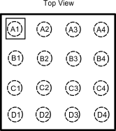
5 Pin Configuration and Functions
YZR Package
16-Pin DSBGA
Top View

Pin Functions
| PIN | TYPE | DESCRIPTION | |
|---|---|---|---|
| NO. | NAME | ||
| A1 | LED1 | Power | High-side current source output for flash LED1 |
| A2, B2 | OUT | Power | Step-up DC-DC converter output. Connect a 10-µF ceramic capacitor between this pin and GND. |
| A3, B3 | SW | Power | Drain connection for internal NMOS and synchronous PMOS switches |
| A4, B4 | GND | Ground | Ground |
| B1 | LED2 | Output | High-side current source output for flash LED2 |
| C1 | LEDI/NTC | Input/Output | Configureable as a high-side current source output for indicator LED or comparator input for LED temperature sensing |
| C2 | TX1/TORCH/GPIO1 | Input/Output | Configureable as a dual-polarity RF power amplifier synchronization input, a hardware torch mode enable, or as a general purpose logic I/O. This pin has an internal 300-kΩ pulldown to GND. |
| C3 | STROBE | Input | Active high hardware flash enable. Drive STROBE high to turn on the flash current pulse. This pin has an internal 300-kΩ pulldown to GND. |
| C4 | IN | Power | Input voltage connection. Connect IN to the input supply, and bypass to GND with a minimum 10-µF or larger ceramic capacitor. |
| D1 | TX2/INT/GPIO2 | Input/Output | Configurable as a dual-polarity power amplifier synchronization input, an interrupt output, or as a general purpose logic I/O. This pin has an internal 300-kΩ pulldown to GND. |
| D2 | SDA | Input/Output | Serial data input output. High impedance in shutdown or in power down. |
| D3 | SCL | Input | Serial clock input. High impedance in shutdown or in power down. |
| D4 | HWEN | Input | Logic high hardware enable. HWEN is a high impedance input and is normally connected with an external pullup resistor to a logic high voltage. |