SNVSAJ9D February 2016 – March 2018 LM36274
PRODUCTION DATA.
- 1 Features
- 2 Applications
- 3 Description
- 4 Revision History
- 5 Pin Configuration and Functions
- 6 Specifications
-
7 Detailed Description
- 7.1 Overview
- 7.2 Functional Block Diagram
- 7.3
Features Description
- 7.3.1 Enabling the LM36274
- 7.3.2 Backlight
- 7.3.3 LCM Bias
- 7.3.4 Software Reset
- 7.3.5 HWEN Input
- 7.3.6 Thermal Shutdown (TSD)
- 7.4 Device Functional Modes
- 7.5 Programming
- 7.6
Register Maps
- 7.6.1 Revision Register (Address = 0x01)[Reset = 0x01]
- 7.6.2 Backlight Configuration1 Register (Address = 0x02)[Reset = 0x28]
- 7.6.3 Backlight Configuration 2 Register (Address = 0x03)[Reset = 0x8D]
- 7.6.4 Backlight Brightness LSB Register (Address = 0x04)[Reset = 0x07]
- 7.6.5 Backlight Brightness MSB Register (Address = 0x05)[Reset = 0xFF]
- 7.6.6 Backlight Auto-Frequency Low Threshold Register (Address = 0x06)[Reset = 0x00]
- 7.6.7 Backlight Auto-Frequency High Threshold Register (Address = 0x07)[Reset = 0x00]
- 7.6.8 Backlight Enable Register (Address = 0x08)[Reset = 0x00]
- 7.6.9 Bias Configuration 1 Register (Address = 0x09)[Reset = 0x18]
- 7.6.10 Bias Configuration 2 register (Address = 0x0A)[Reset = 0x11]
- 7.6.11 Bias Configuration 3 Register (Address = 0x0B)[Reset = 0x00]
- 7.6.12 LCM Boost Bias Register (Address = 0x0C)[Reset = 0x28]
- 7.6.13 VPOS Bias Register (Address = 0x0D)[Reset = 0x1E]
- 7.6.14 VNEG Bias Register (Address = 0x0E)[Reset = 0x1C]
- 7.6.15 Flags Register (Address = 0x0F)[Reset = 0x00]
- 7.6.16 Option 1 Register (Address = 0x10)[Reset = 0x06]
- 7.6.17 Option 2 Register (Address = 0x11)[Reset = 0x35]
- 7.6.18 PWM-to-Digital Code Readback LSB Register (Address = 0x12)[Reset = 0x00]
- 7.6.19 PWM-to-Digital Code Readback MSB Register (Address = 0x13)[Reset = 0x00]
- 8 Application and Implementation
- 9 Power Supply Recommendations
- 10Layout
- 11Device and Documentation Support
- 12Mechanical, Packaging, and Orderable Information
Package Options
Mechanical Data (Package|Pins)
- YFF|24
Thermal pad, mechanical data (Package|Pins)
Orderable Information
7.5.1.5 Addressing Transfer Formats
Each device on the bus has a unique slave address. The LM36274 operates as a slave device with the 7-bit address. If an 8-bit address is used for programming, the 8th bit is 1 for read and 0 for write. The 7-bit address for the device is 0x11.
Before any data is transmitted, the master transmits the address of the slave being addressed. The slave device sends an acknowledge signal on the SDA line, once it recognizes its address. The slave address is the first seven bits after a Start Condition. The direction of the data transfer (R/W) depends on the bit sent after the slave address — the eighth bit.
When the slave address is sent, each device in the system compares this slave address with its own. If there is a match, the device considers itself addressed and sends an acknowledge signal. Depending upon the state of the R/W bit (1: read, 0: write), the device acts as a transmitter or a receiver.
 Figure 45. I2C Device Address
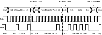
- Master device generates start condition.
- Master device sends slave address (7 bits) and the data direction bit (r/w = 0).
- Slave device sends acknowledge signal if the slave address is correct.
- Master sends control register address (8 bits).
- Slave sends acknowledge signal.
- Master sends data byte to be written to the addressed register.
- Slave sends acknowledge signal.
- If master sends further data bytes the control register address is incremented by one after acknowledge signal.
- Write cycle ends when the master creates stop condition.
Control Register Write Cycle
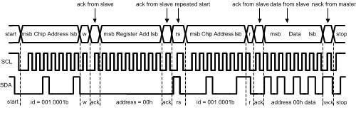
- Master device generates a start condition.
- Master device sends slave address (7 bits) and the data direction bit (r/w = 0).
- Slave device sends acknowledge signal if the slave address is correct.
- Master sends control register address (8 bits).
- Slave sends acknowledge signal
- Master device generates repeated start condition.
- Master sends the slave address (7 bits) and the data direction bit (r/w = 1).
- Slave sends acknowledge signal if the slave address is correct.
- Slave sends data byte from addressed register.
- If the master device sends acknowledge signal, the control register address is incremented by one. Slave device sends data byte from addressed register.
- Read cycle ends when the master does not generate acknowledge signal after data byte and generates stop condition.
Control Register Read Cycle
Table 9. I2C Data Read/Write(1)
| ADDRESS MODE | |
|---|---|
| Data Read | <Start Condition> <Slave Address><r/w =0>[Ack] <Register Addr>[Ack] <Repeated Start Condition> <Slave Address><r/w = 1>[Ack] [Register Data]<Ack or NAck> ...additional reads from subsequent register address possible <Stop Condition> |
| Data Write | <Start Condition> <Slave Address><r/w = 0>[Ack] <Register Addr>[Ack] <Register Data>[Ack] ...additional writes to subsequent register address possible <Stop Condition> |
 Figure 46. Register Write Format
When a READ function is to be accomplished, a WRITE function must precede the READ function, as show in the Read Cycle waveform.
 Figure 47. Register Read Format
NOTE
w = write (SDA = 0), r = read (SDA = 1), ack = acknowledge (SDA pulled down by either master or slave), rs = repeated start id = 7-bit chip address