SNVSCV4 September 2024 LM3645
PRODUCTION DATA
- 1
- 1 Features
- 2 Applications
- 3 Description
- 4 Pin Configuration and Functions
- 5 Specifications
-
6 Detailed Description
- 6.1 Overview
- 6.2 Functional Block Diagram
- 6.3
Feature Description
- 6.3.1 Power Amplifier Synchronization (TORCH/TX)
- 6.3.2 Input Voltage Flash Monitor (IVFM)
- 6.3.3
Fault/Protections
- 6.3.3.1 Fault Operation
- 6.3.3.2 Flash Time-Out
- 6.3.3.3 Overvoltage Protection (OVP)
- 6.3.3.4 Current Limit
- 6.3.3.5 NTC Thermistor Input/Outputs (TEMP1, TEMP2)
- 6.3.3.6 Thermal Scale Back
- 6.3.3.7 Thermal Shutdown (TSD)
- 6.3.3.8 Undervoltage Lockout (UVLO)
- 6.3.3.9 LED and/or VOUT Short Fault
- 6.3.3.10 Fault Behavior Table
- 6.4 Device Functioning Modes
- 6.5 Programming and Control
- 6.6 Register Descriptions
- 7 Application and Implementation
- 8 Power Supply Recommendations
- 9 Layout
- 10Device and Documentation Support
- 11Revision History
- 12Mechanical, Packaging, and Orderable Information
Package Options
Mechanical Data (Package|Pins)
- YCG|25
Thermal pad, mechanical data (Package|Pins)
Orderable Information
6.4.6.3 Output Voltage Regulation
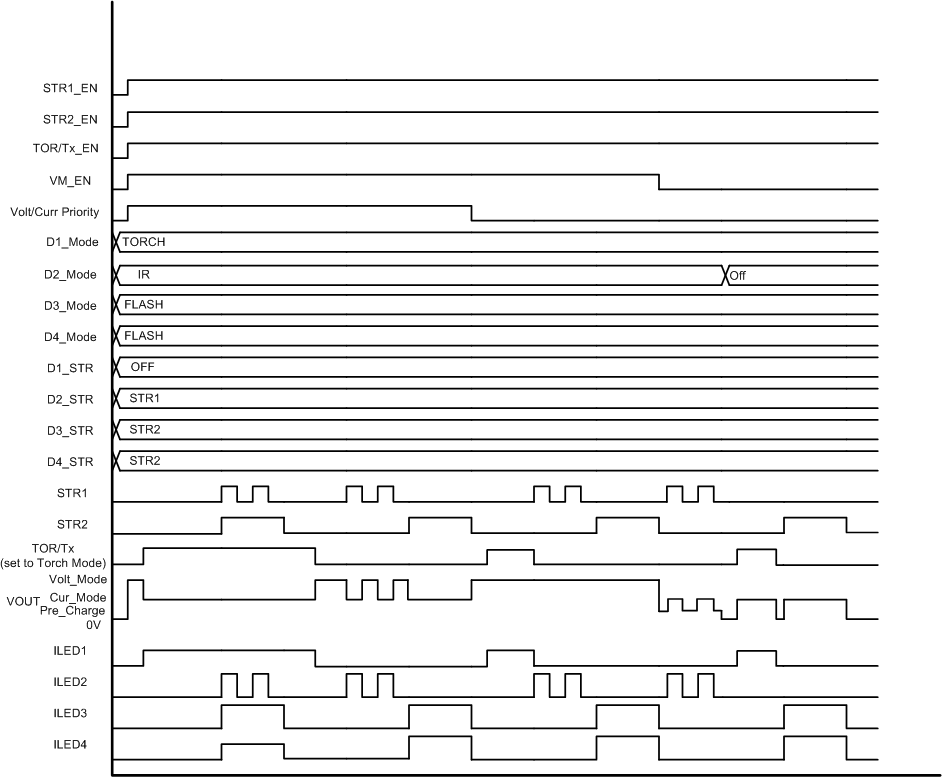
In LED drive mode, the LM3645 boost will either operate in pass mode if the output voltage minus the LED voltage is greater than the target current source headroom voltage. If the output can no longer operate in pass mode, the DC/DC boost will turn on and constantly monitor all enabled outputs and ensure that the output with the highest forward voltage LED always has the correct headroom voltage.
In Voltage drive mode, the output is always regulated to the target value so long as the output voltage is less than the input voltage. If the input voltage is higher than the output voltage, the device will not be regulated and will instead operate in pass mode.
Table 6-2 Output Voltage Assignment Table
| Voltage Mode EN | Output Mode Priority | LED Current On | IR Mode Enabled | Output Level |
|---|---|---|---|---|
| 0 | X | 0 | 0 | Disabled |
| 0 | X | 0 | 1 | Pre-Charge Mode (VOUT = VIN) |
| 0 | X | 1 | X | VOUT = VLED + VHR. Highest enabled LED sets output voltage |
| 1 | 0 | X | X | Output set to regulated voltage specified in voltage mode voltage bits |
| 1 | 1 | 0 | X | Output set to regulated voltage specified in voltage mode voltage bits |
| 1 | 1 | 1 | X | VOUT = VLED + VHR. Highest enabled LED sets output voltage |
 Figure 6-9 Output Voltage and Mode Diagram