SNVSCV4 September   2024 LM3645

PRODUCTION DATA  

  1.   1
  2. Features
  3. Applications
  4. Description
  5. Pin Configuration and Functions
  6. Specifications
    1. 5.1 Absolute Maximum Ratings
    2. 5.2 ESD Ratings
    3. 5.3 Recommended Operating Conditions
    4. 5.4 Thermal Information
    5. 5.5 Electrical Characteristics
    6. 5.6 Timing Requirements
    7. 5.7 Switching Characteristics
    8. 5.8 Typical Characteristics
  7. Detailed Description
    1. 6.1 Overview
    2. 6.2 Functional Block Diagram
    3. 6.3 Feature Description
      1. 6.3.1 Power Amplifier Synchronization (TORCH/TX)
      2. 6.3.2 Input Voltage Flash Monitor (IVFM)
      3. 6.3.3 Fault/Protections
        1. 6.3.3.1  Fault Operation
        2. 6.3.3.2  Flash Time-Out
        3. 6.3.3.3  Overvoltage Protection (OVP)
        4. 6.3.3.4  Current Limit
        5. 6.3.3.5  NTC Thermistor Input/Outputs (TEMP1, TEMP2)
        6. 6.3.3.6  Thermal Scale Back
        7. 6.3.3.7  Thermal Shutdown (TSD)
        8. 6.3.3.8  Undervoltage Lockout (UVLO)
        9. 6.3.3.9  LED and/or VOUT Short Fault
        10. 6.3.3.10 Fault Behavior Table
    4. 6.4 Device Functioning Modes
      1. 6.4.1 Flash Mode
      2. 6.4.2 Torch Mode
      3. 6.4.3 IR Mode
      4. 6.4.4 Voltage Mode
      5. 6.4.5 Mode Transitions
      6. 6.4.6 Boost Operation
        1. 6.4.6.1 Start-Up (Enabling The Device)
        2. 6.4.6.2 Pass Mode
        3. 6.4.6.3 Output Voltage Regulation
    5. 6.5 Programming and Control
      1. 6.5.1 Dx_EN Bits
      2. 6.5.2 STR1 and STR2 Usage
      3. 6.5.3 TOR/TX Usage
      4. 6.5.4 Control State Diagram
      5. 6.5.5 I2C-Compatible Interface
        1. 6.5.5.1 Data Validity
        2. 6.5.5.2 Start and Stop Conditions
        3. 6.5.5.3 Transferring Data
        4. 6.5.5.4 I2C-Compatible Chip Address
    6. 6.6 Register Descriptions
      1. 6.6.1 MainReg Registers
  8. Application and Implementation
    1. 7.1 Application Information
    2. 7.2 Typical Application
      1. 7.2.1 Design Requirements
      2. 7.2.2 Output Control Examples
        1. 7.2.2.1 Four Channel Flash with Strobe1 Trigger Starting in Standby
        2. 7.2.2.2 Four Channel Flash with Strobe1 Trigger Starting in I2C Torch
        3. 7.2.2.3 Mixed Mode Functionality
        4. 7.2.2.4 Voltage Mode Only
        5. 7.2.2.5 Voltage Mode With Advanced IR
      3. 7.2.3 Detailed Design Procedure
        1. 7.2.3.1 Snubber Requirement
        2. 7.2.3.2 Output Capacitor Selection
        3. 7.2.3.3 Input Capacitor Selection
        4. 7.2.3.4 Inductor Selection
      4. 7.2.4 Application Curves
  9. Power Supply Recommendations
  10. Layout
    1. 9.1 Layout Guidelines
    2. 9.2 Layout Example
  11. 10Device and Documentation Support
    1. 10.1 Third-Party Products Disclaimer
    2. 10.2 Receiving Notification of Documentation Updates
    3. 10.3 Support Resources
    4. 10.4 Trademarks
    5. 10.5 Electrostatic Discharge Caution
    6. 10.6 Glossary
  12. 11Revision History
  13. 12Mechanical, Packaging, and Orderable Information

Package Options

Mechanical Data (Package|Pins)
Thermal pad, mechanical data (Package|Pins)
Orderable Information

Typical Characteristics

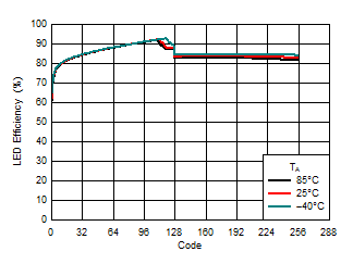
ICL = 5 A

LM3645 Flash Efficiency vs Code Tri-Temp
VIN = 3.3 VfSW = 4 MHz
Figure 5-2 Flash Efficiency vs Code Tri-Temp
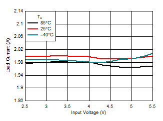
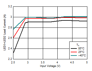
LM3645 Flash Current vs. Input Voltage
ILOAD = 2 AfSW = 4 MHz
Figure 5-4 Flash Current vs. Input Voltage
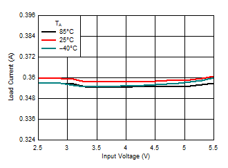
LM3645 Torch Current vs. Input Voltage
ILOAD = 360 mAfSW = 4 MHz
Figure 5-6 Torch Current vs. Input Voltage
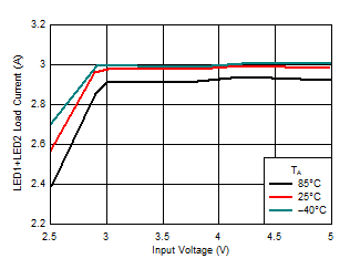
LM3645 Flash Line Regulation
ILOAD = 3 AfSW = 2 MHz
two outputs tied
Figure 5-8 Flash Line Regulation
LM3645 Flash Load Regulation
VIN = 3.3 VfSW = 2 MHz
two outputs tied
Figure 5-10 Flash Load Regulation
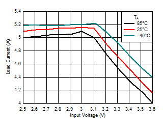
LM3645 Current Limit
two outputs tiedfSW = 2 MHz
Figure 5-12 Current Limit
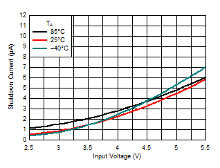
LM3645 Shutdown Current
VEN = VQC = 0 V
Figure 5-14 Shutdown Current
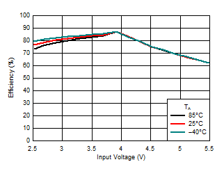
LM3645 Flash Efficiency vs Line Tri-Temp
ILOAD = 2 AfSW = 4 MHz
Figure 5-3 Flash Efficiency vs Line Tri-Temp
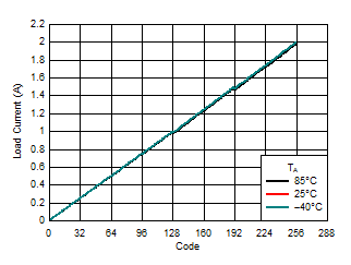
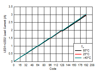
LM3645 Flash Current vs. Code
VIN = 3.3 VfSW = 4 MHz
Figure 5-5 Flash Current vs. Code
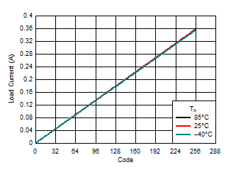
LM3645 Torch Current vs. Code
VIN = 3.3 VfSW = 4 MHz
Figure 5-7 Torch Current vs. Code
LM3645 Flash Line Regulation
ILOAD = 3 AfSW = 4 MHz
two outputs tied
Figure 5-9 Flash Line Regulation
LM3645 Flash Load Regulation
VIN = 3.3 VfSW = 4 MHz
two outputs tied
Figure 5-11 Flash Load Regulation
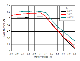
LM3645 Current Limit
two outputs tiedfSW = 4 MHz
Figure 5-13 Current Limit
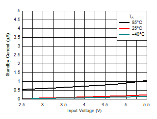
LM3645 Standby Current
VEN = VQC = 1.8 V
Figure 5-15 Standby Current