SNVS449O June   2007  – April 2015 LM3668

PRODUCTION DATA.  

  1. Features
  2. Applications
  3. Description
  4. Revision History
  5. Device Comparison Table
  6. Pin Configuration and Functions
  7. Specifications
    1. 7.1 Absolute Maximum Ratings
    2. 7.2 ESD Ratings
    3. 7.3 Recommended Operating Conditions
    4. 7.4 Thermal Information
    5. 7.5 Electrical Characteristics
    6. 7.6 Typical Characteristics
  8. Detailed Description
    1. 8.1 Overview
    2. 8.2 Functional Block Diagram
    3. 8.3 Feature Description
      1. 8.3.1 Buck Operation
      2. 8.3.2 Boost Operation
      3. 8.3.3 Internal Synchronous Rectification
      4. 8.3.4 Current Limit Protection
      5. 8.3.5 Undervoltage Protection
      6. 8.3.6 Short Circuit Protection
      7. 8.3.7 Shutdown
      8. 8.3.8 Thermal Shutdown
      9. 8.3.9 Start-Up
    4. 8.4 Device Functional Modes
      1. 8.4.1 PWM Operation
      2. 8.4.2 PFM Operation
  9. Application and Implementation
    1. 9.1 Application Information
      1. 9.1.1 MODE/SYNC Pin
      2. 9.1.2 VSEL Pin
    2. 9.2 Typical Application
      1. 9.2.1 Design Requirements
        1. 9.2.1.1 Maximum Current
      2. 9.2.2 Detailed Design Procedure
        1. 9.2.2.1 Inductor Selection
        2. 9.2.2.2 Input Capacitor Selection
        3. 9.2.2.3 Output Capacitor Selection
      3. 9.2.3 Application Curves
  10. 10Power Supply Recommendations
  11. 11Layout
    1. 11.1 Layout Guidelines
    2. 11.2 Layout Example
  12. 12Device and Documentation Support
    1. 12.1 Device Support
      1. 12.1.1 Third-Party Products Disclaimer
      2. 12.1.2 Documentation Support
        1. 12.1.2.1 Related Documentation
    2. 12.2 Trademarks
    3. 12.3 Electrostatic Discharge Caution
    4. 12.4 Glossary
  13. 13Mechanical, Packaging, and Orderable Information

Package Options

Mechanical Data (Package|Pins)
Thermal pad, mechanical data (Package|Pins)
Orderable Information

11 Layout

11.1 Layout Guidelines

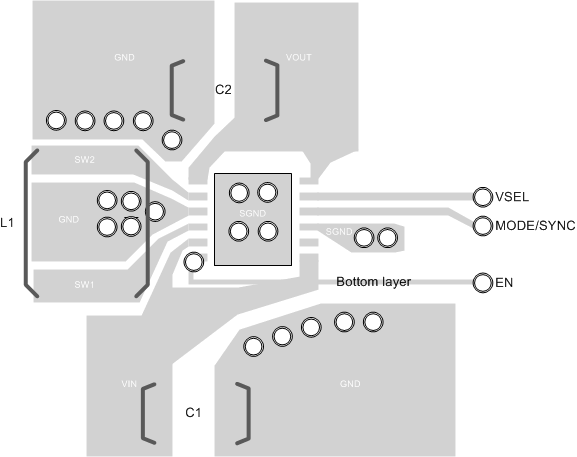
As for any high frequency switcher, it is important to place the external components as close as possible to the IC to maximize device performance. Below are some layout recommendations:

  1. Place input filter and output filter capacitors close to the IC to minimize copper trace resistance which will directly effect the overall ripple voltage.
  2. Route noise sensitive trace away from noisy power components. Separate power GND (Noisy GND) and Signal GND (quiet GND) and star GND them at a single point on the PCB preferably close to device GND.
  3. Connect the ground pins and filter capacitors together via a ground plane to prevent switching current circulating through the ground plane. Additional layout consideration regarding the WSON package can be found in AN-1187 Leadless Leadframe Package (LLP), SNOA401.

11.2 Layout Example
LM3668 layout.gif