SNVS294S November   2004  – May 2016 LM3671 , LM3671-Q1

PRODUCTION DATA.  

  1. Features
  2. Applications
  3. Description
  4. Revision History
  5. Pin Configuration and Functions
  6. Specifications
    1. 6.1 Absolute Maximum Ratings
    2. 6.2 ESD Ratings: LM3671
    3. 6.3 ESD Ratings: LM3671-Q1
    4. 6.4 Recommended Operating Conditions
    5. 6.5 Thermal Information
    6. 6.6 Dissipation Ratings
    7. 6.7 Electrical Characteristics
    8. 6.8 Typical Characteristics
  7. Detailed Description
    1. 7.1 Overview
    2. 7.2 Functional Block Diagram
    3. 7.3 Feature Description
      1. 7.3.1 Circuit Operation
      2. 7.3.2 Soft Start
    4. 7.4 Device Functional Modes
      1. 7.4.1 PWM Operation
        1. 7.4.1.1 Internal Synchronous Rectification
        2. 7.4.1.2 Current Limiting
      2. 7.4.2 PFM Operation
      3. 7.4.3 Shutdown
      4. 7.4.4 Low Dropout Operation (LDO)
  8. Application and Implementation
    1. 8.1 Application Information
    2. 8.2 Typical Application
      1. 8.2.1 Typical Application: Fixed-Voltage Version
        1. 8.2.1.1 Design Requirements
        2. 8.2.1.2 Detailed Design Procedure
          1. 8.2.1.2.1 Inductor Selection
            1. 8.2.1.2.1.1 Method 1
            2. 8.2.1.2.1.2 Method 2
          2. 8.2.1.2.2 Input Capacitor Selection
          3. 8.2.1.2.3 Output Capacitor Selection
        3. 8.2.1.3 Application Curves
      2. 8.2.2 Typical Application: ADJ Version
        1. 8.2.2.1 Design Requirements
        2. 8.2.2.2 Detailed Design Procedure
          1. 8.2.2.2.1 Output Voltage Selection for LM3671-ADJ
        3. 8.2.2.3 Application Curves
  9. Power Supply Recommendations
  10. 10Layout
    1. 10.1 Layout Guidelines
    2. 10.2 Layout Example
    3. 10.3 DSBGA Package Assembly and Use
  11. 11Device and Documentation Support
    1. 11.1 Device Support
      1. 11.1.1 Third-Party Products Disclaimer
    2. 11.2 Documentation Support
      1. 11.2.1 Related Documentation
    3. 11.3 Related Links
    4. 11.4 Community Resources
    5. 11.5 Trademarks
    6. 11.6 Electrostatic Discharge Caution
    7. 11.7 Glossary
  12. 12Mechanical, Packaging, and Orderable Information

Package Options

Mechanical Data (Package|Pins)
Thermal pad, mechanical data (Package|Pins)
Orderable Information

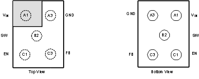
5 Pin Configuration and Functions

DBV Package
5 Pin SOT-23
Top View
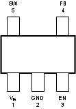
LM3671 LM3671-Q1 20108402.gif
NKH Package
6-Pin USON
LM3671 LM3671-Q1 20108462.gif
YZR Package
5-Pin DSBGA
LM3671 LM3671-Q1 20108444.gif

Pin Functions

PIN TYPE DESCRIPTION
LM3671, LM3671-Q1 LM3671 NAME
SOT-23 DSBGA USON
1 A1 3 VIN Power Power supply input. Connect to the input filter capacitor (see Input Capacitor Selection).
2 A3 2 GND Ground Ground pin.
3 C1 1 EN Digital Enable pin. The device is in shutdown mode when voltage to this pin is < 0.4 V and enabled when > 1 V. Do not leave this pin floating.
4 C3 6 FB Analog Feedback analog input. Connect directly to the output filter capacitor for fixed voltage versions. For adjustable version external resistor dividers are required (see Typical Application: ADJ Version). The internal resistor dividers are disabled for the adjustable version.
5 B2 4 SW Analog Switching node connection to the internal PFET switch and NFET synchronous rectifier.
5 SGND Ground Signal ground (feedback ground).