SNVS434M July 2006 – November 2016 LM3673
PRODUCTION DATA.
- 1 Features
- 2 Applications
- 3 Description
- 4 Revision History
- 5 Voltage Options
- 6 Pin Configuration and Functions
- 7 Specifications
- 8 Detailed Description
- 9 Application and Implementation
- 10Power Supply Recommendations
- 11Layout
- 12Device and Documentation Support
- 13Mechanical, Packaging, and Orderable Information
Package Options
Mechanical Data (Package|Pins)
- YZR|5
Thermal pad, mechanical data (Package|Pins)
Orderable Information
1 Features
- 16-µA Typical Quiescent Current
- 350-mA Maximum Load Capability
- 2-MHz PWM Fixed Switching Frequency (Typical)
- Automatic PFM/PWM Mode Switching
- Available in Fixed and Adjustable Output Voltages
- Internal Synchronous Rectification for High Efficiency
- Internal Soft Start
- 0.01-µA Typical Shutdown Current
- Operates From a Single Li-Ion Cell Battery
- Current Overload and Thermal Shutdown Protection
- Only Three Tiny Surface-Mount External Components Required (One Inductor, Two Ceramic Capacitors)
2 Applications
- Mobile Phones
- PDAs
- MP3 Players
- W-LAN
- Portable Instruments
- Digital Still Cameras
- Portable Hard Disk Drives
3 Description
The LM3673 step-down DC-DC converter is optimized for powering low voltage circuits from a single Li-Ion cell battery and input voltage rails from 2.7 V to 5.5 V. It provides up to 350-mA load current over the entire input voltage range. There are several different fixed voltage output options available, as well as an adjustable output voltage version ranging from 1.1 V to 3.3 V.
The device offers superior features and performance for mobile phones and similar portable systems. The LM3673 uses intelligent automatic switching between pulse width modulation (PWM) and pulse frequency modulation (PFM) for better efficiency. During PWM mode, the device operates at a fixed-frequency of
2 MHz (typical). Hysteretic PFM mode extends the battery life by reducing the quiescent current to 16 µA (typical) during light load and standby operation. Internal synchronous rectification provides high efficiency during PWM mode operation. In shutdown mode, the device turns off and reduces battery consumption to 0.01 µA (typical).
The LM3673 is available in a tiny 5-pin DSBGA package. A high switching frequency of 2 MHz (typical) allows the use of three tiny surface-mount components: an inductor and two ceramic capacitors.
Device Information(1)
| PART NUMBER | PACKAGE | BODY SIZE (MAX) |
|---|---|---|
| LM3673 | DSBGA (5) | 1.413 mm × 1.083 mm |
- For all available packages, see the orderable addendum at the end of the data sheet.
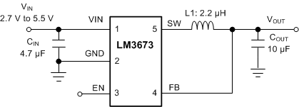
Typical Application Circuit

Typical Application Circuit for ADJ Version
