SNVS520F August 2008 – November 2016 LM3686
PRODUCTION DATA.
- 1 Features
- 2 Applications
- 3 Description
- 4 Revision History
- 5 Description (Continued)
- 6 Pin Configuration and Functions
-
7 Specifications
- 7.1 Absolute Maximum Ratings
- 7.2 ESD Ratings
- 7.3 Recommended Operating Conditions
- 7.4 Thermal Information
- 7.5 Electrical Characteristics: Linear Regulator - LILO
- 7.6 Electrical Characteristics: Linear Regulator - LDO
- 7.7 Electrical Characteristics: DC-DC Converter
- 7.8 Electrical Characteristics: Global Parameters (DCDC, LILO, and LDO)
- 7.9 Typical Characteristics
- 8 Detailed Description
- 9 Application and Implementation
- 10Power Supply Recommendations
- 11Layout
- 12Device and Documentation Support
- 13Mechanical, Packaging, and Orderable Information
Package Options
Mechanical Data (Package|Pins)
- YZR|12
Thermal pad, mechanical data (Package|Pins)
Orderable Information
6 Pin Configuration and Functions
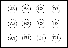
YZR Package
12-Pin DSBGA
Top View

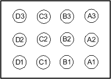
YZR Package
12-Pin DSBGA
Bottom View

Pin Functions
| PIN | TYPE | DESCRIPTION | |
|---|---|---|---|
| NO. | NAME | ||
| A1 | PGND | Ground | Power ground pin |
| A2 | SW | Analog | Switching node connection to the internal PFET switch and NFET synchronous rectifier. |
| A3 | FB_DCDC | Input | Feedback analog input for the DC-DC converter. Connect to the output filter capacitor. |
| B1 | VBATT | Power | Power supply input for switcher. Connect to the input filter capacitor. |
| B2 | EN_LILO | Input | Enable input for the linear regulator. The linear regulator is in shutdown mode if voltage at this pin is < 0.4 V and enabled if > 1.1 V. Do not leave this pin floating. |
| B3 | EN_DCDC | Input | Enable input for the DC-DC converter. The DC-DC converter is in shutdown mode if voltage at this pin is < 0.4 V and enabled if > 1.1 V. Do not leave this pin floating. |
| C1 | VIN_LDO | Input | Input power to LDO — must tie to VBATT at all times. |
| C2 | EN_LDO | Input | Enable input for the linear regulator. The linear regulator is in shutdown mode if voltage at this pin is < 0.4 V and enabled if > 1.1 V. Do not leave this pin floating. |
| C3 | QGND | Ground | Quiet GND pin for LDO and reference circuit |
| D1 | VOUT_LDO | Output | Voltage output of the linear regulator |
| D2 | VOUT_LILO | Output | Voltage output of the low input linear regulator |
| D3 | VIN_LILO | Input | Input power to LILO (VIN_LILO) connects to output of DCDC or standalone. |