SNVSAF2A February 2016 – February 2016 LM36922H
PRODUCTION DATA.
- 1 Features
- 2 Applications
- 3 Description
- 4 Revision History
- 5 Pin Configuration and Functions
- 6 Specifications
-
7 Detailed Description
- 7.1 Overview
- 7.2 Functional Block Diagram
- 7.3 Feature Description
- 7.4
Device Functional Modes
- 7.4.1 Brightness Control Modes
- 7.4.2 Boost Switching Frequency
- 7.4.3 Auto-Switching Frequency
- 7.4.4 I2C Address Select (ASEL)
- 7.4.5
Fault Protection/Detection
- 7.4.5.1
Overvoltage Protection (OVP)
- 7.4.5.1.1 Case 1 OVP Fault Only (OVP Threshold Hit and All Enabled Current Sink Inputs > 40 mV)
- 7.4.5.1.2 Case 2a OVP Fault and Open LED String Fault (OVP Threshold Occurrence and Any Enabled Current Sink Input ≤ 40 mV)
- 7.4.5.1.3 Case 2b OVP Fault and Open LED String Fault (OVP Threshold Duration and Any Enabled Current Sink Input ≤ 40 mV)
- 7.4.5.1.4 OVP/LED Open Fault Shutdown
- 7.4.5.1.5 Testing for LED String Open
- 7.4.5.2 Voltage Limitations on LED1, LED2
- 7.4.5.3 LED String Short Fault
- 7.4.5.4 Overcurrent Protection (OCP)
- 7.4.5.5 Device Overtemperature
- 7.4.5.1
Overvoltage Protection (OVP)
- 7.5 Programming
- 7.6 Register Maps
- 8 Applications and Implementation
- 9 Power Supply Recommendations
- 10Layout
- 11Device and Documentation Support
- 12Mechanical, Packaging, and Orderable Information
Package Options
Mechanical Data (Package|Pins)
- YFF|12
Thermal pad, mechanical data (Package|Pins)
Orderable Information
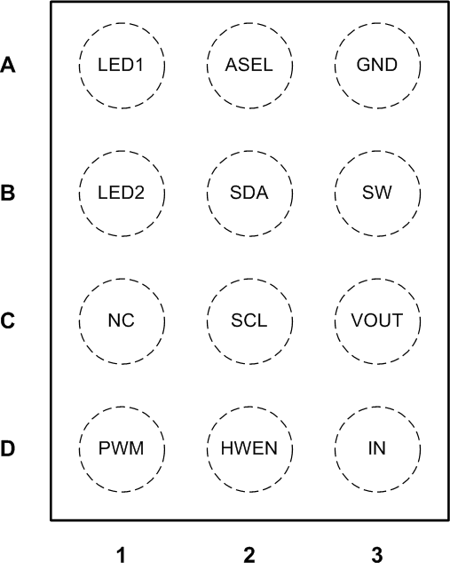
5 Pin Configuration and Functions
YFF Package
12-Pin DSBGA
Top View

Pin Functions
| PIN | I/O | DESCRIPTION | |
|---|---|---|---|
| NUMBER | NAME | ||
| A1 | LED1 | Input | Input to current sink 1. The boost converter regulates the minimum voltage between LED1, LED2 to VHR. |
| A2 | ASEL | Input | ASEL is a logic input which selects between two I2C address options. This pin is read on power up (VIN going above 1.8 V, and HWEN going above a logic high voltage). GND = address 0x36, logic high = address 0x37. |
| A3 | GND | Input | Ground |
| B1 | LED2 | Input | Input pin to current sink 2. The boost converter regulates the minimum voltage between LED1, LED2 to VHR. |
| B2 | SDA | I/O | Data I/O for I2C-Compatible Interface. |
| B3 | SW | Output | Drain connection for internal low side NFET, and anode connection for external Schottky diode. |
| C1 | NC | Input | Unused pin. Connect externally to GND. |
| C2 | SCL | Input | Clock input for I2C-compatible interface. |
| C3 | OUT | Input | OUT serves as the sense point for overvoltage protection. Connect OUT to the positive pin of the output capacitor. |
| D1 | PWM | Input | Logic level input for PWM current control. |
| D2 | HWEN | Input | Hardware enable input. Drive HWEN high to bring the device out of shutdown and allow I2C writes or PWM control. |
| D3 | IN | Input | Input voltage connection. Bypass IN to GND with a minimum 2.2-µF ceramic capacitor. |