SNOSDA4D June 2020 – November 2023 LM339LV , LM393LV , TL331LV , TL391LV
PRODMIX
- 1
- 1 Features
- 2 Applications
- 3 Description
- 4 Pin Configuration and Functions
-
5 Specifications
- 5.1 Absolute Maximum Ratings
- 5.2 ESD Ratings
- 5.3 Recommended Operating Conditions
- 5.4 Thermal Information for TL3x1LV
- 5.5 Thermal Information, LM393LV
- 5.6 Thermal Information, LM339LV
- 5.7 Electrical Characteristics, TL3x1LV
- 5.8 Switching Characteristics, TL3x1LV
- 5.9 Electrical Characteristics, LM393LV
- 5.10 Switching Characteristics, LM393LV
- 5.11 Electrical Characteristics, LM339LV
- 5.12 Switching Characteristics, LM339LV
- 5.13 Typical Characteristics
- 6 Detailed Description
-
7 Application and Implementation
- 7.1 Application Information
- 7.2 Typical Applications
- 7.3 Power Supply Recommendations
- 7.4 Layout
- 8 Device and Documentation Support
- 9 Revision History
- 10Mechanical, Packaging, and Orderable Information
Package Options
Mechanical Data (Package|Pins)
Thermal pad, mechanical data (Package|Pins)
- DSG|8
Orderable Information
7.2.4 Time Delay Generator
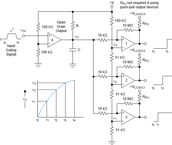
The circuit shown in Figure 7-13 provides output signals at a prescribed time interval from a time reference and automatically resets the output low when the input returns to 0V. This is useful for sequencing a "power on" signal to trigger a controlled start-up of power supplies.
 Figure 7-13 Time Delay Generator
Consider the case of VIN = 0. The output of comparator 4 is also at ground, "shorting" the capacitor and holding it at 0V. This implies that the outputs of comparators 1, 2, and 3 are also at 0V. When an input signal is applied, the output of open drain comparator 4 goes High-Z and C charges exponentially through R. This is indicated in the graph. The output voltages of comparators 1, 2, and 3 switch to the high state in sequence when VC rises above the reference voltages V1, V2 and V3. A small amount of hysteresis has been provided by the 10 kΩ and 10 MΩ resistors to insure fast switching when the RC time constant is chosen to give long delay times. A good starting point is R = 100 kΩ and C = 0.01 µF to 1 µF.
All outputs will immediately go low when VIN falls to 0V, due to the comparator output going low and immediately discharging the capacitor.
Comparator 4 must be a open-drain type output (TLV902x), whereas comparators 1 though 3 may be either open drain or push-pull output, depending on system requirements. RPU is not required for push-pull output devices.