SNVS114G May 1999 – February 2015 LM3940
PRODUCTION DATA.
- 1 Features
- 2 Applications
- 3 Description
- 4 Revision History
- 5 Pin Configuration and Functions
- 6 Specifications
- 7 Detailed Description
- 8 Application and Implementation
- 9 Power Supply Recommendations
- 10Layout
- 11Device and Documentation Support
- 12Mechanical, Packaging, and Orderable Information
Package Options
Mechanical Data (Package|Pins)
Thermal pad, mechanical data (Package|Pins)
Orderable Information
7 Detailed Description
7.1 Overview
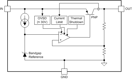
The LM3940 is a low dropout regulator capable of sourcing a 1-A load. The LM3940 provides 3.3 V from 5-V supply. LM3940 is ideally suited for system which contain both 5-V and 3.3-V logic, with prime power provided from a 5-V bus.
7.2 Functional Block Diagram

7.3 Feature Description
7.3.1 Output Voltage Accuracy
Output voltage accuracy specifies minimum and maximum output voltage error, relative to the expected nominal output voltage. This accuracy error includes the errors introduced by line and load regulation across the full range of rated load and line operating conditions, unless otherwise specified by the Electrical Characteristics.
7.3.2 Short-Circuit Protection
The internal current limit circuit is used to protect the LDO against high-load current faults or shorting events. During a current-limit event, the LDO sources constant current. Therefore, the output voltage falls when load impedance decreases. Note also that if a current limit occurs and the resulting output voltage is low, excessive power may be dissipated across the LDO, resulting in a thermal shutdown of the output.
7.3.3 Thermal Protection
The LM3940 contains a thermal shutdown protection circuit to turn off the output current when excessive heat is dissipated in the LDO. The thermal time-constant of the semiconductor die is fairly short, and thus the output cycles on and off at a high rate when thermal shutdown is reached until the power dissipation is reduced.
The internal protection circuit of LM3940 is designed to protect against thermal overload conditions. The circuit is not intended to replace proper heat sinking. Continuously running the device into thermal shutdown degrades its reliability.
7.4 Device Functional Modes
7.4.1 Operation with VIN = 5 V
The device operates at input voltage is 5 V and output voltage is 3.3 V. The LM3940 is a true low dropout regulator, it can hold its 3.3-V output in regulation with input voltages as low as 4.5 V.