SNVS114G May 1999 – February 2015 LM3940
PRODUCTION DATA.
- 1 Features
- 2 Applications
- 3 Description
- 4 Revision History
- 5 Pin Configuration and Functions
- 6 Specifications
- 7 Detailed Description
- 8 Application and Implementation
- 9 Power Supply Recommendations
- 10Layout
- 11Device and Documentation Support
- 12Mechanical, Packaging, and Orderable Information
Package Options
Mechanical Data (Package|Pins)
Thermal pad, mechanical data (Package|Pins)
Orderable Information
10 Layout
10.1 Layout Guidelines
For best overall performance, place all the circuit components on the same side of the circuit board and as near as practical to the respective LDO pin connections. Place ground return connections to the input and output capacitor, and to the LDO ground pin as close to each other as possible, connected by a wide, component-side, copper surface. The use of vias and long traces to create LDO circuit connections is strongly discouraged and negatively affects system performance. This grounding and layout scheme minimizes inductive parasitic, and thereby reduces load-current transients, minimizes noise, and increases circuit stability.
A ground reference plane is also recommended and is either embedded in the PCB itself or located on the bottom side of the PCB opposite the components. This reference plane serves to assure accuracy of the output voltage, shield noise, and behaves similar to a thermal plane to spread heat from the LDO device. In most applications, this ground plane is necessary to meet thermal requirements.
10.2 Layout Example
 Figure 15. LM3940 Layout Example
10.3 Heatsinking
A heatsink may be required depending on the maximum power dissipation and maximum ambient temperature of the application. Under all possible operating conditions, the junction temperature must be within the range specified under Absolute Maximum Ratings.
To determine if a heatsink is required, the power dissipated by the regulator, PD, must be calculated.
Figure 16 shows the voltages and currents which are present in the circuit, as well as the formula for calculating the power dissipated in the regulator:

PD = (VIN − VOUT) IOUT + (VIN) IG
The next parameter which must be calculated is the maximum allowable temperature rise, TR(max). This is calculated by using the formula:
TR (max) = TJ (max) − TA (max)
-
Where: TJ (max)is the maximum allowable junction temperature, which is 125°C for commercial grade parts.
-
TA (max)is the maximum ambient temperature which will be encountered in the application.
Using the calculated values for TR(max) and PD, the maximum allowable value for the junction-to-ambient thermal resistance, Rθ(JA), can now be found:
Rθ(JA) = TR (max)/PD
IMPORTANT: If the maximum allowable value for θ(JA) is found to be ≥ 23.3°C/W for the TO-220 package, ≥ 40.9°C/W for the DDPAK/TO-263 package, or ≥59.3°C/W for the SOT-223 package, no heatsink is needed since the package alone will dissipate enough heat to satisfy these requirements.
If the calculated value for θ(JA)falls below these limits, a heatsink is required.
10.3.1 Heatsinking TO-220 Package Parts
The TO-220 can be attached to a typical heatsink, or secured to a copper plane on a PC board. If a copper plane is to be used, the values of Rθ(JA) will be the same as shown in the Heatsinking DDPAK/TO-263 and SOT-223 Package Parts section for the DDPAK/TO-263.
If a manufactured heatsink is to be selected, the value of heatsink-to-ambient thermal resistance, Rθ(H−A), must first be calculated:
Rθ(H−A) = Rθ(JA) − Rθ(C−H) − Rθ(J−C)
-
Where: Rθ(J−C)is defined as the thermal resistance from the junction to the surface of the case. A value of 4°C/W can be assumed for θ(J−C) for this calculation.
-
Rθ(C−H)is defined as the thermal resistance between the case and the surface of the heatsink. The value of θ(C−H) will vary from about 1.5°C/W to about 2.5°C/W (depending on method of attachment, insulator, etc.). If the exact value is unknown, 2°C/W should be assumed for θ(C−H).
When a value for Rθ(H−A) is found using the equation shown above, a heatsink must be selected that has a value that is less than or equal to this number.
Rθ(H−A) is specified numerically by the heatsink manufacturer in the catalog, or shown in a curve that plots temperature rise vs. power dissipation for the heatsink.
10.3.2 Heatsinking DDPAK/TO-263 and SOT-223 Package Parts
Both the DDPAK/TO-263 (KTT) and SOT-223 (DCY) packages use a copper plane on the PCB and the PCB itself as a heatsink. To optimize the heat sinking ability of the plane and PCB, solder the tab of the package to the plane.
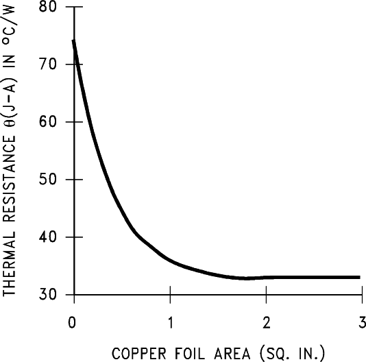
Figure 17 shows for the DDPAK/TO-263 the measured values of Rθ(JA) for different copper area sizes using a typical PCB with 1 ounce copper and no solder mask over the copper area used for heatsinking.
 Figure 17. Rθ(JA) vs. Copper (1 ounce) Area for the DDPAK/TO-263 Package
As shown in Figure 17, increasing the copper area beyond 1 square inch produces very little improvement. It should also be observed that the minimum value of Rθ(JA) for the DDPAK/TO-263 package mounted to a PCB is 32°C/W.
As a design aid, Figure 18 shows the maximum allowable power dissipation compared to ambient temperature for the DDPAK/TO-263 device (assuming Rθ(JA) is 35°C/W and the maximum junction temperature is 125°C).
 Figure 18. Maximum Power Dissipation vs. TAMB for the DDPAK/TO-263 Package
Figure 19 and Figure 20 show the information for the SOT-223 package. Figure 20 assumes a Rθ(JA) of 74°C/W for 1 ounce copper and 51°C/W for 2 ounce copper and a maximum junction temperature of 125°C.
 Figure 19. Rθ(JA) vs. Copper (2 ounce) Area for the SOT-223 Package
Please see AN-1028 Maximum Power Enhancement Techniques for Power Packages, SNVA036 for power enhancement techniques to be used with the SOT-223 package.
