SLOS456O January 2005 – June 2024
PRODUCTION DATA
- 1
- 1 Features
- 2 Applications
- 3 Description
- 4 Device Comparison Table
- 5 Pin Configuration and Functions
-
6 Specifications
- 6.1 Absolute Maximum Ratings
- 6.2 ESD Ratings
- 6.3 Recommended Operating Conditions
- 6.4 Thermal Information
- 6.5 LM4040A20I, LM4040B20I Electrical Characteristics
- 6.6 LM4040C20I, LM4040D20I Electrical Characteristics
- 6.7 LM4040C20Q, LM4040D20Q Electrical Characteristics
- 6.8 LM4040A25I, LM4040B25I Electrical Characteristics
- 6.9 LM4040C25I, LM4040D25I Electrical Characteristics
- 6.10 LM4040C25Q, LM4040D25Q Electrical Characteristics
- 6.11 LM4040A30I, LM4040B30I Electrical Characteristics
- 6.12 LM4040C30I, LM4040D30I Electrical Characteristics
- 6.13 LM4040C30Q, LM4040D30Q Electrical Characteristics
- 6.14 LM4040A41I, LM4040B41I Electrical Characteristics
- 6.15 LM4040C41I, LM4040D41I Electrical Characteristics
- 6.16 LM4040A50I, LM4040B50I Electrical Characteristics
- 6.17 LM4040C50I, LM4040D50I Electrical Characteristics
- 6.18 LM4040C50Q, LM4040D50Q Electrical Characteristics
- 6.19 LM4040A82I, LM4040B82I Electrical Characteristics
- 6.20 LM4040C82I, LM4040D82I Electrical Characteristics
- 6.21 LM4040A10I, LM4040B10I Electrical Characteristics
- 6.22 LM4040C10I, LM4040D10I Electrical Characteristics
- 6.23 Typical Characteristics
- 7 Detailed Description
- 8 Applications and Implementation
- 9 Device and Documentation Support
- 10Revision History
- 11Mechanical, Packaging, and Orderable Information
Package Options
Mechanical Data (Package|Pins)
Thermal pad, mechanical data (Package|Pins)
Orderable Information
3 Description
The LM4040 series of shunt voltage references are versatile, easy-to-use references that cater to a vast array of applications. The 2-pin fixed-output device requires no external capacitors for operation and is stable with all capacitive loads. Additionally, the reference offers low dynamic impedance, low noise, and low temperature coefficient to maintain a stable output voltage over a wide range of operating currents and temperatures. The LM4040 uses fuse and Zener-zap reverse breakdown voltage trim during wafer sort to offer four output voltage tolerances, ranging from 0.1% (maximum) for the A grade to 1% (maximum) for the D grade. Thus, a great deal of flexibility is offered to designers in choosing the best cost-to-performance ratio for their applications.
Packaged in space-saving SC-70 and SOT-23-3 packages and requiring a minimum current of 45μA (typical), the LM4040 also is ideal for portable applications. The LM4040xI is characterized for operation over an ambient temperature range of –40°C to 85°C. The LM4040xQ is characterized for operation over an ambient temperature range of –40°C to 125°C.
| PART NUMBER | PACKAGE (PIN)(1) | BODY SIZE (NOM) (2) |
|---|---|---|
| LM4040 | SOT-23 (3) | 2.92mm × 1.30mm |
| SC70 (6) | 2.00mm × 1.25mm |
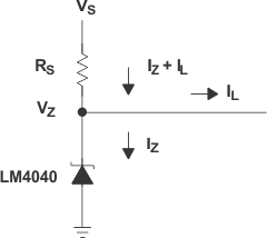
 Simplified Schematic