SNVS049F February 2000 – March 2016 LM4120
PRODUCTION DATA.
- 1 Features
- 2 Applications
- 3 Description
- 4 Revision History
- 5 Pin Configuration and Functions
- 6 Specifications
- 7 Detailed Description
- 8 Application and Implementation
- 9 Power Supply Recommendations
- 10Layout
- 11Device and Documentation Support
- 12Mechanical, Packaging, and Orderable Information
Package Options
Mechanical Data (Package|Pins)
- DBV|5
Thermal pad, mechanical data (Package|Pins)
Orderable Information
6 Specifications
6.1 Absolute Maximum Ratings
over operating free-air temperature range (unless otherwise noted) (1)| MIN | MAX | UNIT | ||
|---|---|---|---|---|
| Maximum voltage on input or enable pins | –0.3 | 14 | V | |
| Output short-circuit duraion | Indefinite | |||
| Power dissipation (TA = 25°C) (2) | 350 | mW | ||
| Lead temperature | Soldering, (10 sec.) | 260 | °C | |
| Vapor Phase (60 sec.) | 215 | °C | ||
| Infrared (15 sec.) | 220 | °C | ||
| Storage temperature, Tstg | –65 | 150 | °C | |
(1) Stresses beyond those listed under Absolute Maximum Ratings may cause permanent damage to the device. These are stress ratings only, which do not imply functional operation of the device at these or any other conditions beyond those indicated under Recommended Operating Conditions. Exposure to absolute-maximum-rated conditions for extended periods may affect device reliability.
(2) Without PCB copper enhancements. The maximum power dissipation must be derated at elevated temperatures and is limited by TJMAX (maximum junction temperature), RθJA (junction-to-ambient thermal resistance) and TA (ambient temperature). The maximum power dissipation at any temperature is: PDissMAX = (TJMAX – TA) / RθJA up to the value listed in the Absolute Maximum Ratings.
6.2 ESD Ratings
| VALUE | UNIT | |||
|---|---|---|---|---|
| V(ESD) | Electrostatic discharge | Human body model (HBM), per ANSI/ESDA/JEDEC JS-001(1) | ±2000 | V |
| Charged device model (CDM), per JEDEC specification JESD22-C101(2) | ±750 | |||
| Machine Model | ±200 | |||
(1) JEDEC document JEP155 states that 500-V HBM allows safe manufacturing with a standard ESD control process.
(2) JEDEC document JEP157 states that 250-V CDM allows safe manufacturing with a standard ESD control process.
6.3 Recommended Operating Conditions
over operating free-air temperature range (unless otherwise noted)| MIN | NOM | MAX | UNIT | |
|---|---|---|---|---|
| Ambient temperature | –40 | 85 | °C | |
| Junction temperature | –40 | 125 | °C |
6.4 Thermal Information
| THERMAL METRIC(1) | LM4120 | UNIT | |
|---|---|---|---|
| DBV [SOT-23] | |||
| 5 PINS | |||
| RθJA | Junction-to-ambient thermal resistance | 170.4 | °C/W |
| RθJC(top) | Junction-to-case (top) thermal resistance | 123.9 | °C/W |
| RθJB | Junction-to-board thermal resistance | 30.4 | °C/W |
| ψJT | Junction-to-top characterization parameter | 17.2 | °C/W |
| ψJB | Junction-to-board characterization parameter | 29.9 | °C/W |
(1) For more information about traditional and new thermal metrics, see the Semiconductor and IC Package Thermal Metrics application report, SPRA953.
6.5 Electrical Characteristics
unless otherwise specified, VIN = 3.3 V, ILOAD = 0, COUT = 0.01 µF, TA = Tj = 25°C.| PARAMETER | TEST CONDITIONS | MIN (1) | TYP (2) | MAX (1) | UNIT | ||
|---|---|---|---|---|---|---|---|
| 1.8 V, 2.048 V, AND 2.5 V | |||||||
| VOUT | Output voltage initial accuracy LM4120A-1.800 LM4120A-2.048 LM4120A-2.500 |
±0.2% | |||||
| LM4120-1.800 LM4120-2.048 LM4120-2.500 |
±0.5% | ||||||
| TCVOUT/°C | Temperature coefficient | –40°C ≤ TA ≤ +125°C | 14 | 50 | ppm/°c | ||
| ΔVOUT/ΔVIN | Line regulation | 3.3 V ≤ VIN ≤ 12 V | 0.0007 | 0.008 | %/V | ||
| –40°C ≤ TA ≤ 85°C | 0.01 | ||||||
| ΔVOUT/ΔILOAD | Load regulation | 0 mA ≤ ILOAD ≤ 1 mA | 0.03 | 0.08 | %/mA | ||
| –40°C ≤ TA ≤ 85°C | 0.17 | ||||||
| 1 mA ≤ ILOAD ≤ 5 mA | 0.01 | 0.04 | |||||
| –40°C ≤ TA ≤ 85°C | 0.1 | ||||||
| –1 mA ≤ ILOAD ≤ 0 mA | 0.04 | 0.12 | |||||
| –5 mA ≤ ILOAD ≤ −1 mA | 0.01 | ||||||
| VIN−VOUT | Dropout voltage (3) | ILOAD = 0 mA | 45 | 65 | mV | ||
| –40°C ≤ TA ≤ 85°C | 80 | ||||||
| ILOAD = 1 mA | 120 | 150 | |||||
| –40°C ≤ TA ≤ 85°C | 180 | ||||||
| ILOAD = 5 mA | 180 | 210 | |||||
| –40°C ≤ TA ≤ 85°C | 250 | ||||||
| VN | Output(4) | 0.1 Hz to 10 Hz | 20 | µVPP | |||
| 10 Hz to 10 kHz | 36 | ||||||
| IS | Supply current | 160 | 250 | µA | |||
| –40°C ≤ TA ≤ 85°C | 275 | ||||||
| ISS | Power-down supply current | Enable = 0.4 V –40°C ≤ TJ ≤ 85°C Enable = 0.2 V |
1 | µA | |||
| –40°C ≤ TA ≤ 85°C | 2 | ||||||
| VH | Logic high input voltage | 2.4 | V | ||||
| –40°C ≤ TA ≤ 85°C | 2.4 | ||||||
| VL | Logic low input voltage | 0.4 | V | ||||
| –40°C ≤ TA ≤ 85°C | 0.2 | ||||||
| IH | Logic high input current | 7 | µA | ||||
| –40°C ≤ TA ≤ 85°C | 15 | ||||||
| IL | Logic low input current | 0.1 | µA | ||||
| ISC | Short circuit current | VIN = 3.3 V, VOUT = 0 | 15 | mA | |||
| –40°C ≤ TA ≤ 85°C | 6 | 30 | |||||
| VIN = 12 V, VOUT = 0 | 17 | ||||||
| –40°C ≤ TA ≤ 85°C | 6 | 30 | |||||
| Hyst | Thermal hysteresis (5) | –40°C ≤ TA ≤ 125°C | 0.5 | mV/V | |||
| ΔVOUT | Long term stability (6) | 1000 hrs @ 25°C | 100 | ppm | |||
| 3 V, 3.3 V, 4.096 V, AND 5 V | |||||||
| VOUT | Output voltage initial accuracy LM4120A-3.000 LM4120A-3.300 LM4120A-4.096 LM4120A-5.000 |
±0.2% | |||||
| LM4120-3.000 LM4120-3.300 LM4120-4.096 LM4120-5.000 |
±0.5% | ||||||
| TCVOUT/°C | Temperature coefficient | –40°C ≤ TA ≤ 125°C | 14 | 50 | ppm/°c | ||
| ΔVOUT/ΔVIN | Line regulation | (VOUT + 1 V) ≤ VIN ≤ 12 V | 0.0007 | 0.008 | %/V | ||
| –40°C ≤ TA ≤ 85°C | 0.01 | ||||||
| ΔVOUT/ΔILOAD | Load regulation | 0 mA ≤ ILOAD ≤ 1 mA | 0.03 | 0.08 | %/mA | ||
| –40°C ≤ TA ≤ 85°C | 0.17 | ||||||
| 1 mA ≤ ILOAD ≤ 5 mA | 0.01 | 0.04 | |||||
| –40°C ≤ TA ≤ 85°C | 0.1 | ||||||
| –1 mA ≤ ILOAD ≤ 0 mA | 0.04 | 0.12 | |||||
| –5 mA ≤ ILOAD ≤ –1 mA | 0.01 | ||||||
| VIN−VOUT | Dropout voltage (3) | ILOAD = 0 mA | 45 | 65 | mV | ||
| –40°C ≤ TA ≤ 85°C | 80 | ||||||
| ILOAD = 1 mA | 120 | 150 | |||||
| –40°C ≤ TA ≤ 85°C | 180 | ||||||
| ILOAD = 5 mA | 180 | 210 | |||||
| –40°C ≤ TA ≤ 85°C | 250 | ||||||
| 3 V, 3.3 V, 4.096 V, AND 5 V (continued) | |||||||
| VN | Output noise voltage(4) | 0.1 Hz to 10 Hz | 20 | µVPP | |||
| 10 Hz to 10 kHz | 36 | ||||||
| IS | Supply current | 160 | 250 | µA | |||
| –40°C ≤ TA ≤ 85°C | 275 | ||||||
| ISS | Power-down supply current | Enable = 0.4 V –40°C ≤ TJ ≤ 85°C Enable = 0.2 V |
1 | µA | |||
| –40°C ≤ TA ≤ 85°C | 2 | ||||||
| VH | Logic high input voltage | 2.4 | V | ||||
| –40°C ≤ TA ≤ 85°C | 2.4 | ||||||
| VL | Logic low input voltage | 0.4 | V | ||||
| –40°C ≤ TA ≤ 85°C | 0.2 | ||||||
| IH | Logic high input current | 7 | µA | ||||
| –40°C ≤ TA ≤ 85°C | 15 | ||||||
| IL | Logic low input current | 0.1 | µA | ||||
| ISC | Short circuit current | VOUT = 0 | 15 | mA | |||
| –40°C ≤ TA ≤ 85°C | 6 | 30 | |||||
| VIN = 12 V, VOUT = 0 | 17 | ||||||
| –40°C ≤ TA ≤ 85°C | 6 | 30 | |||||
| Hyst | Thermal hysteresis (5) | –40°C ≤ TA ≤ 125°C | 0.5 | mV/V | |||
| ΔVOUT | Long term stability (6) | 1000 hours @ 25°C | 100 | ppm | |||
(1) Limits are 100% production tested at 25°C. Limits over the operating temperature range are ensured through correlation using Statistical Quality Control (SQC) methods. The limits are used to calculate TI's Averaging Outgoing Quality Level (AOQL).
(2) Typical numbers are at 25°C and represent the most likely parametric norm.
(3) Dropout voltage is the differential voltage between VOUT and VIN at which VOUT changes ≤ 1% from VOUT at VIN = 3.3 V for 1.8 V, 2 V, 2.5 V, and VOUT + 1 V for others. For 1.8-V option, dropout voltage is not ensured over temperature. A parasitic diode exists between input and output pins; it will conduct if VOUT is pulled to a higher voltage than VIN.
(4) Output noise voltage is proportional to VOUT. VN for other voltage option is calculated using (VN(1.8 V) / 1.8) × VOUT.
VN (2.5 V) = (36 μVPP / 1.8) × 2.5 = 46 μVPP.
VN (2.5 V) = (36 μVPP / 1.8) × 2.5 = 46 μVPP.
(5) Thermal hysteresis is defined as the change in 25°C output voltage before and after exposing the device to temperature extremes.
(6) Long term stability is change in VREF at 25°C measured continuously during 1000 hours.
6.6 Typical Characteristics
unless otherwise specified, VIN = 3.3 V, VOUT = 2.5 V, ILOAD = 0, COUT = 0.022 µF, TA = 25°C, and VEN = VIN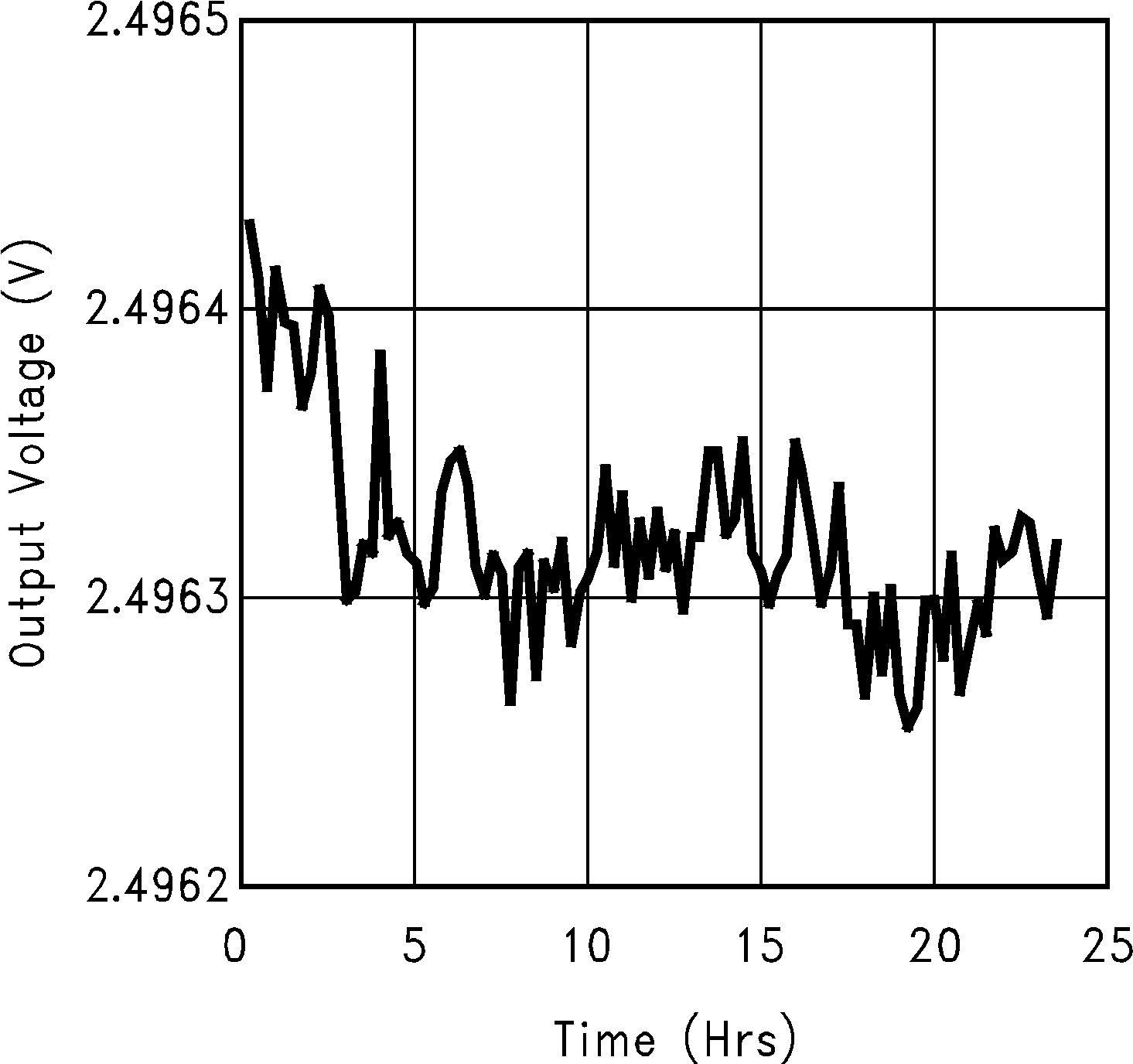 Figure 1. Long Term Drift
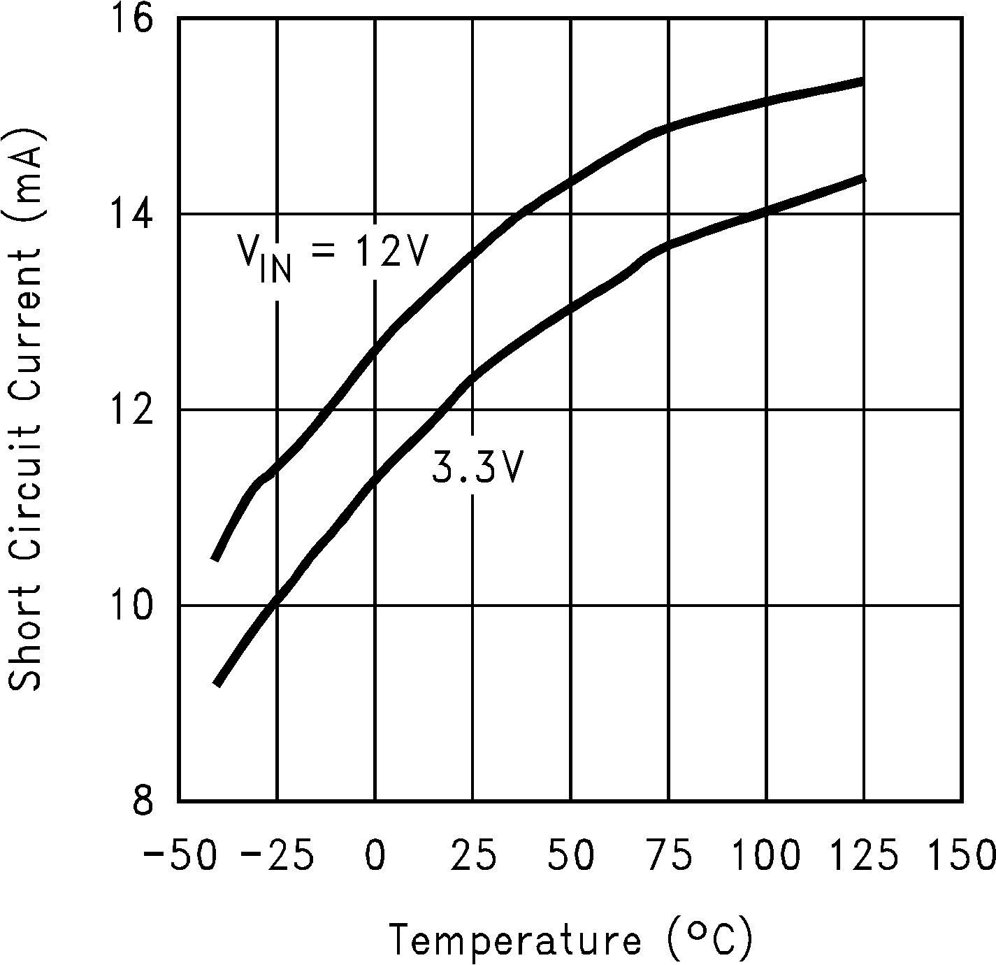 Figure 3. Short Circuit Current vs Temperature
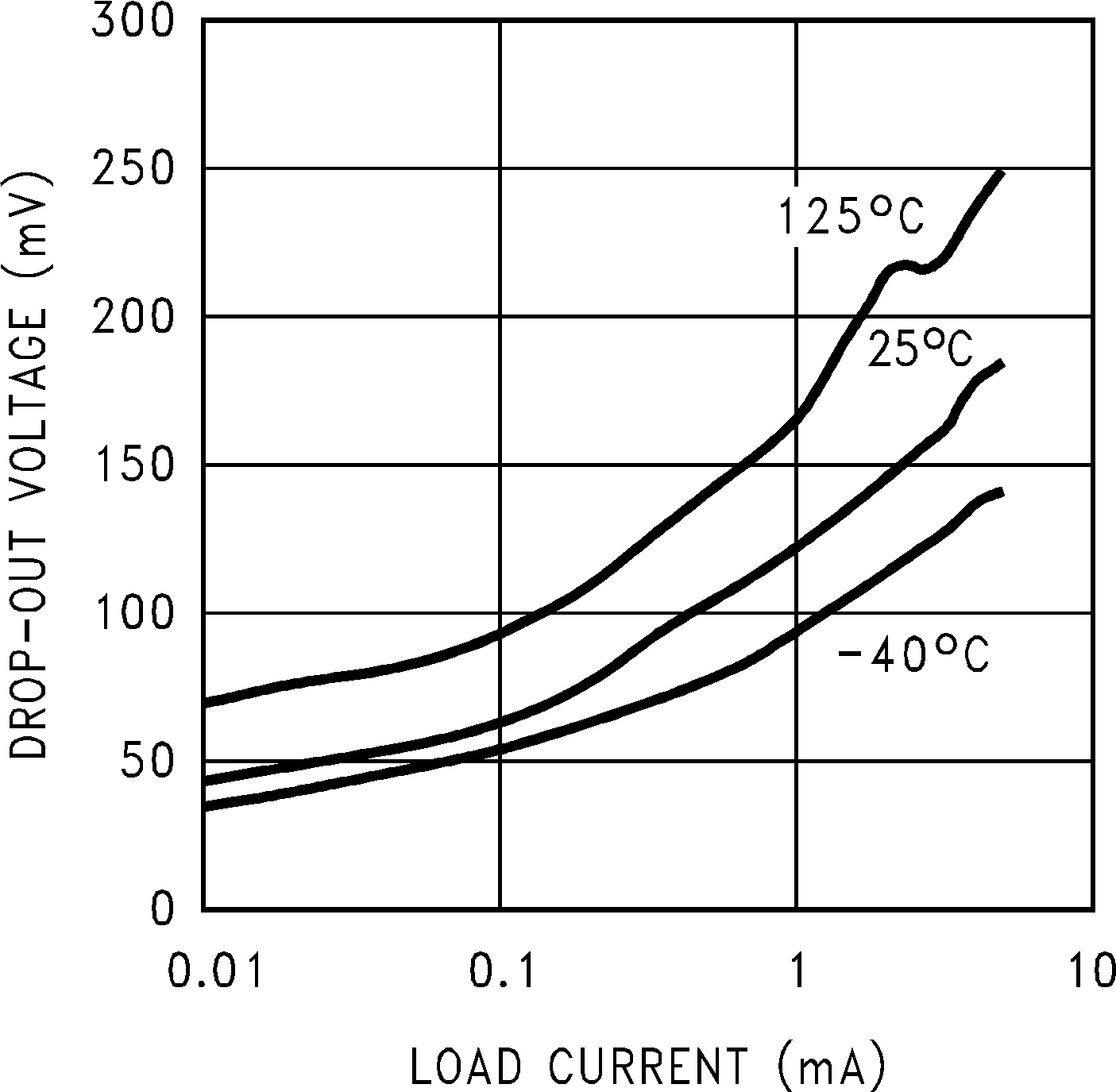 Figure 5. Dropout Voltage vs Load Current
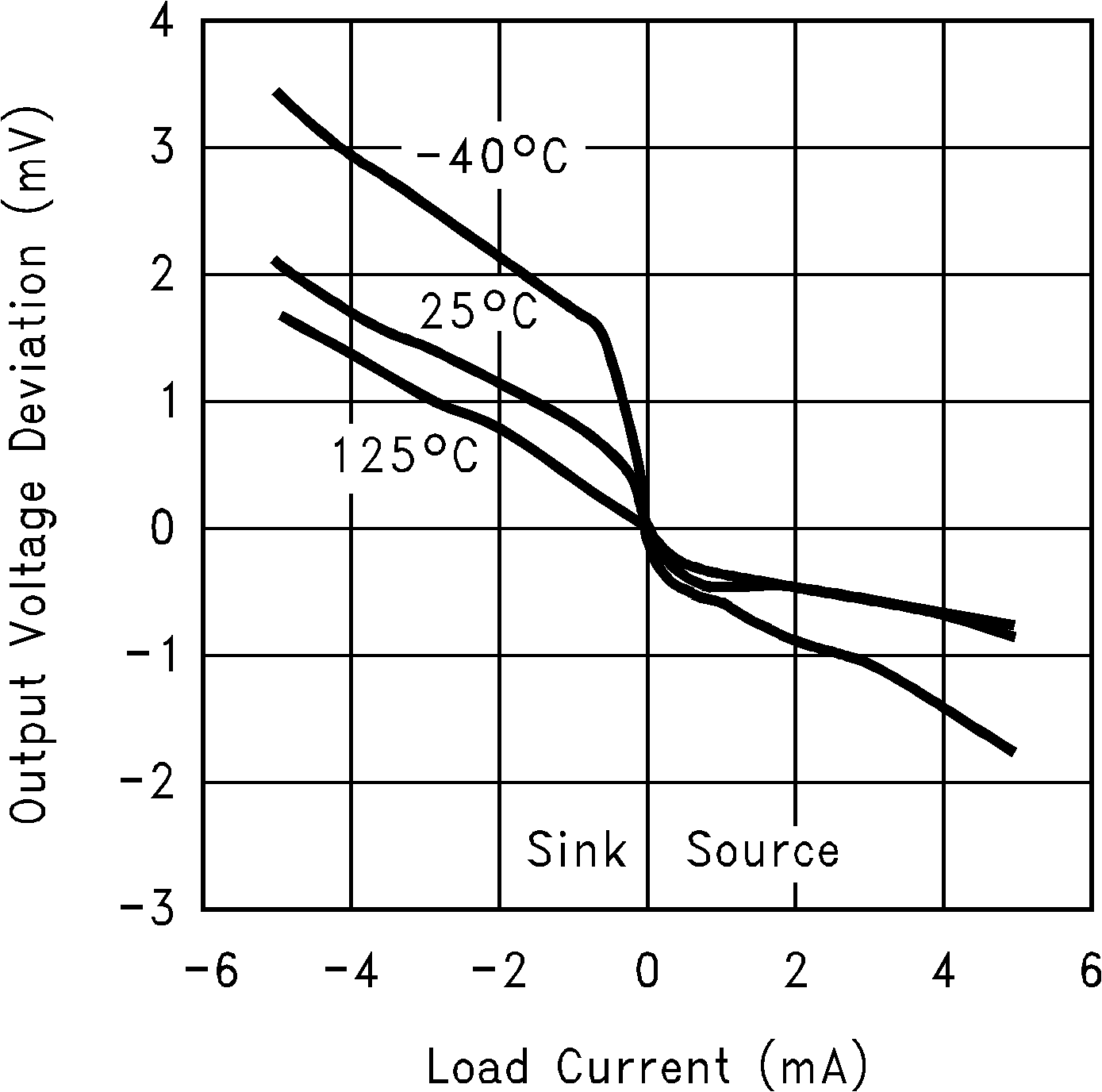 Figure 7. Load Regulation
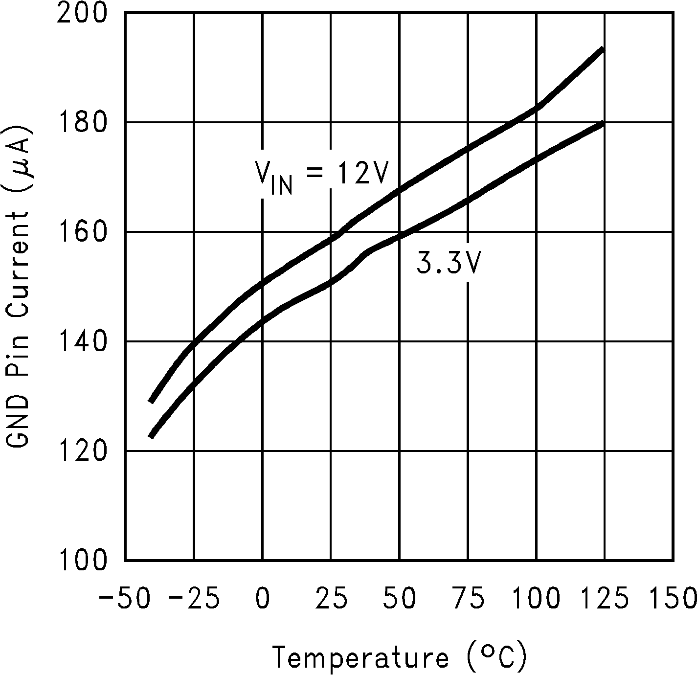 Figure 9. GND Pin Current at No Load vs Temperature
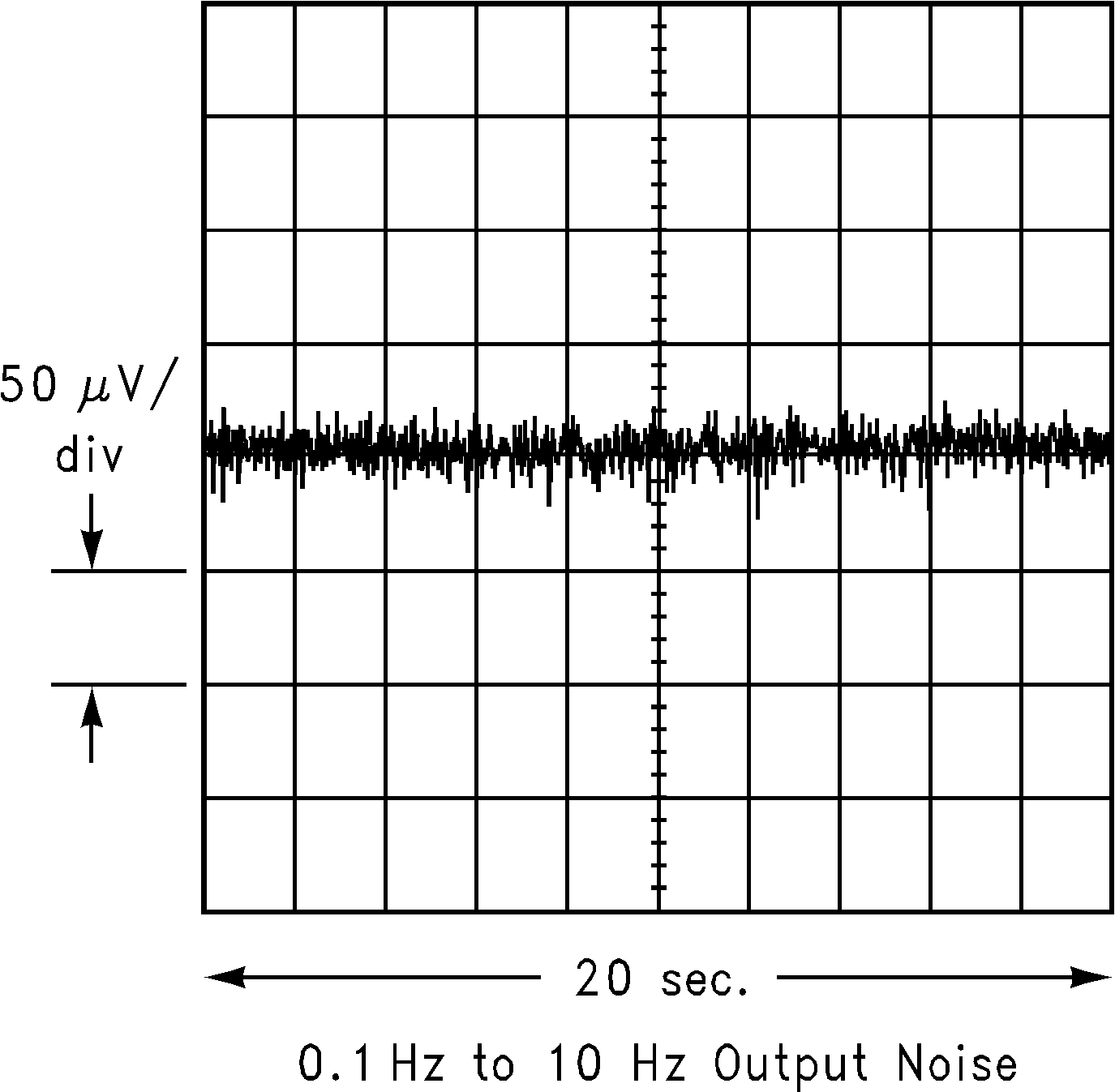 Figure 11. 0.1-Hz to 10-Hz Output Noise
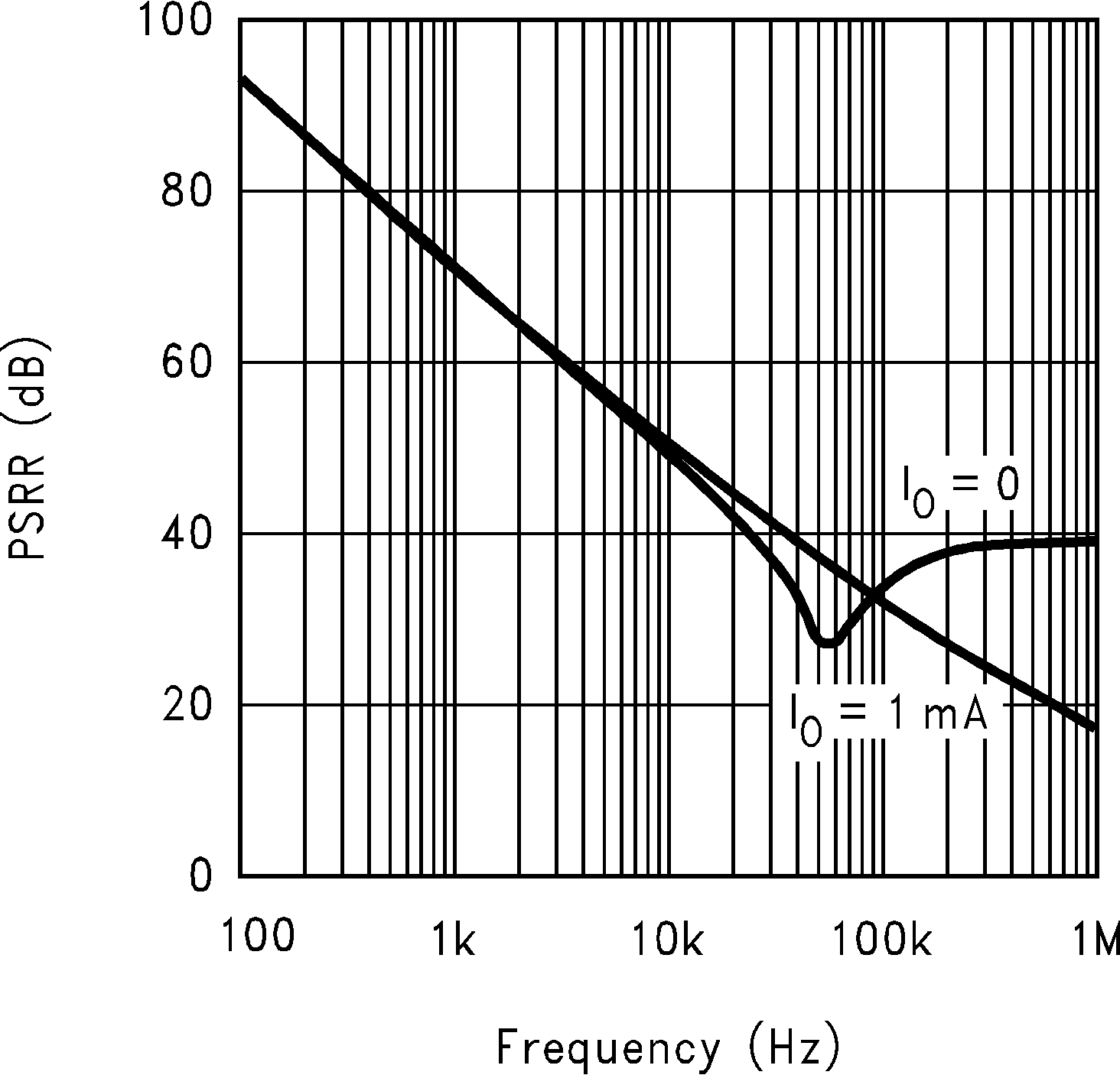 Figure 13. PSRR vs Frequency
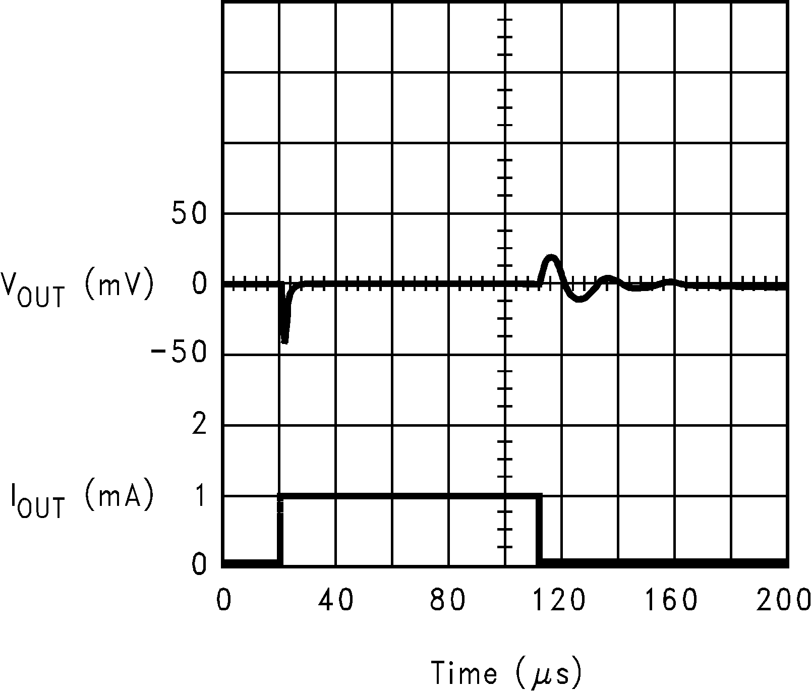 Figure 15. Load Step Response
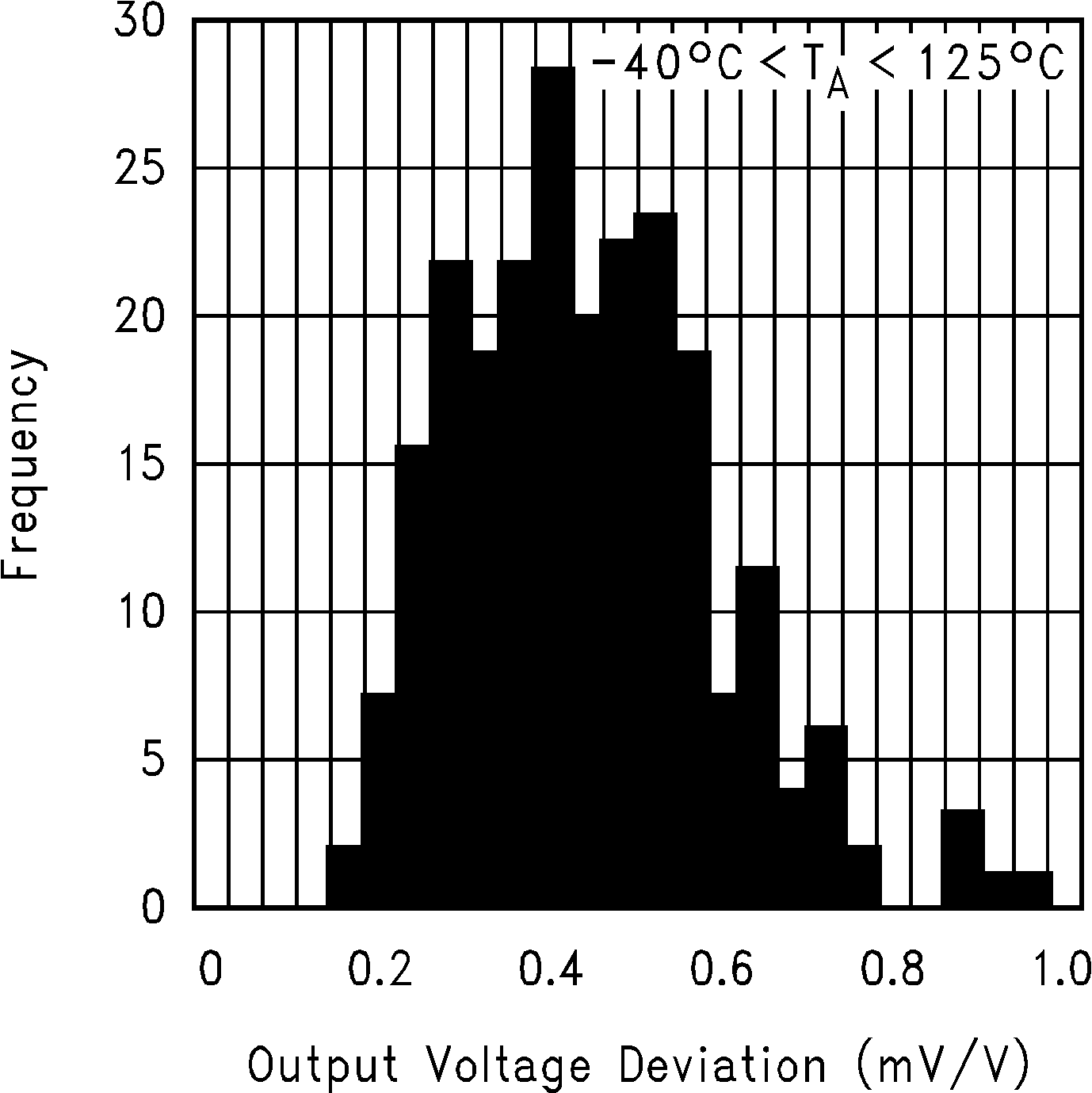 Figure 17. Thermal Hysteresis
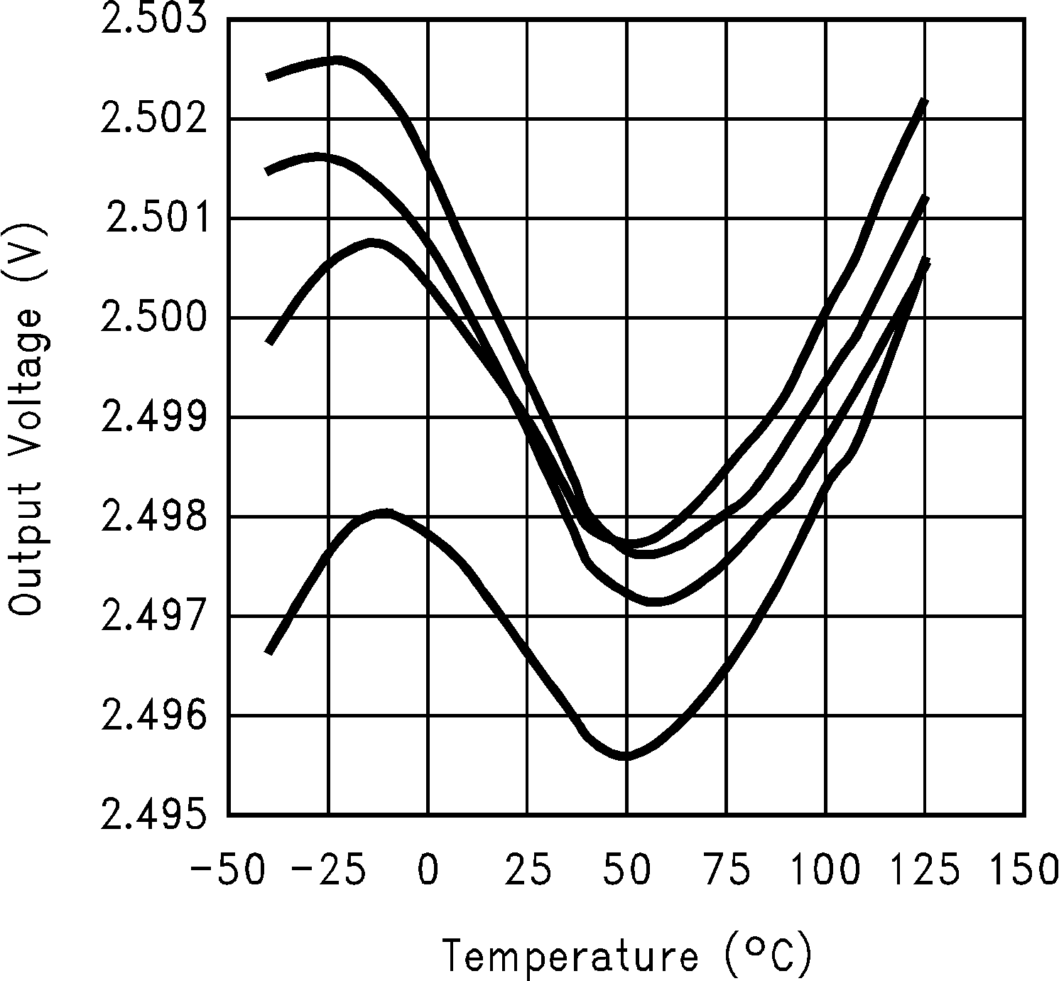 Figure 2. Typical Temperature Drift
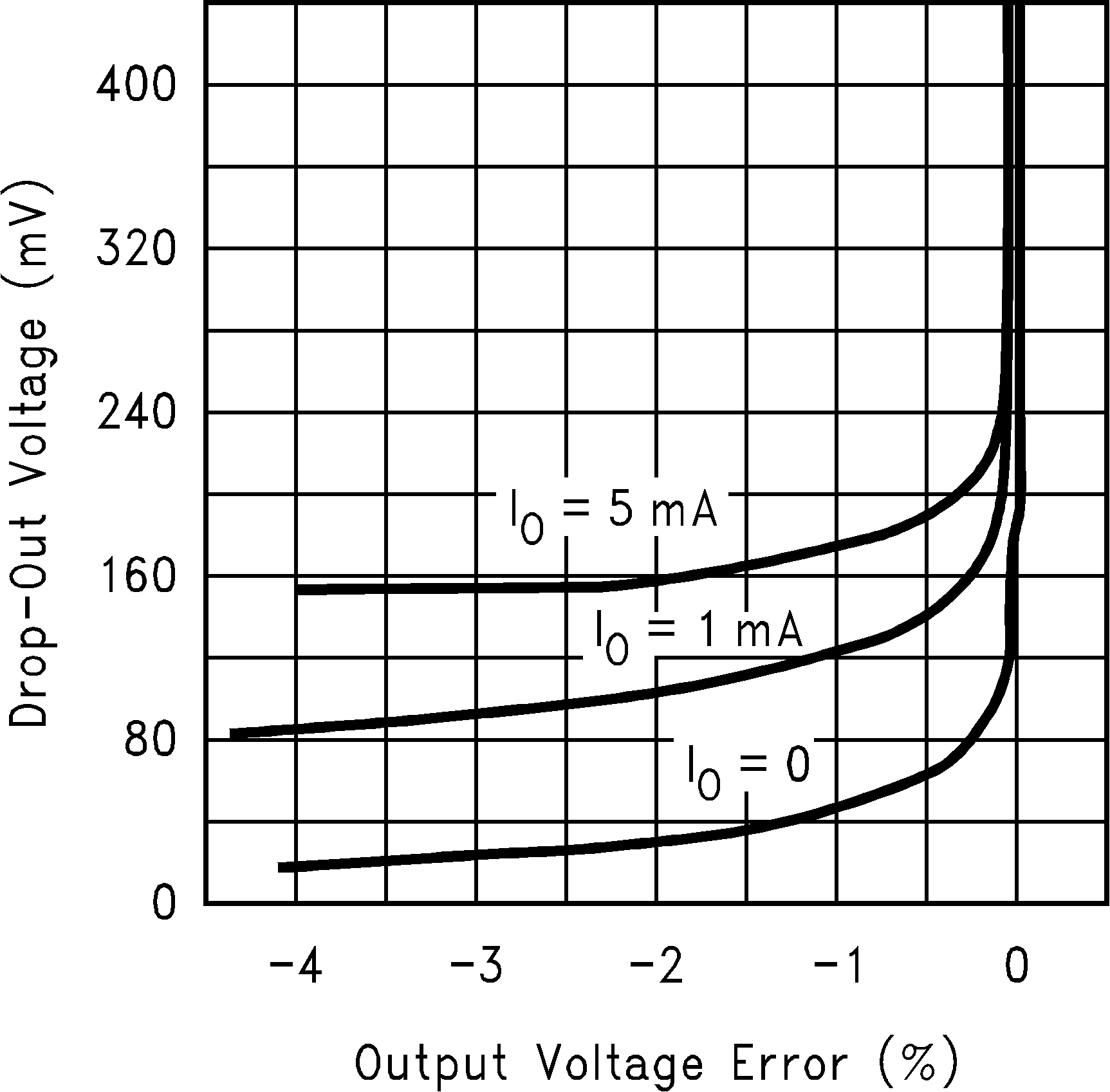 Figure 4. Dropout Voltage vs Output Error
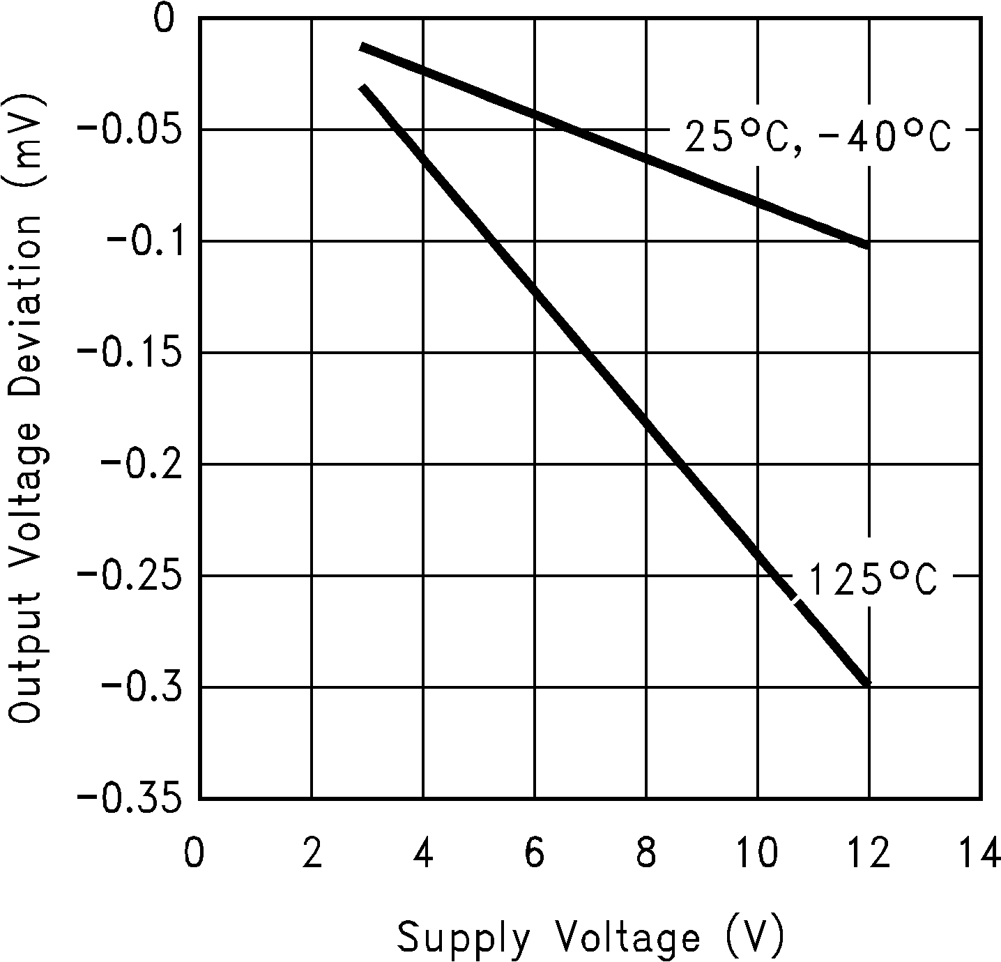 Figure 6. Line Regulation
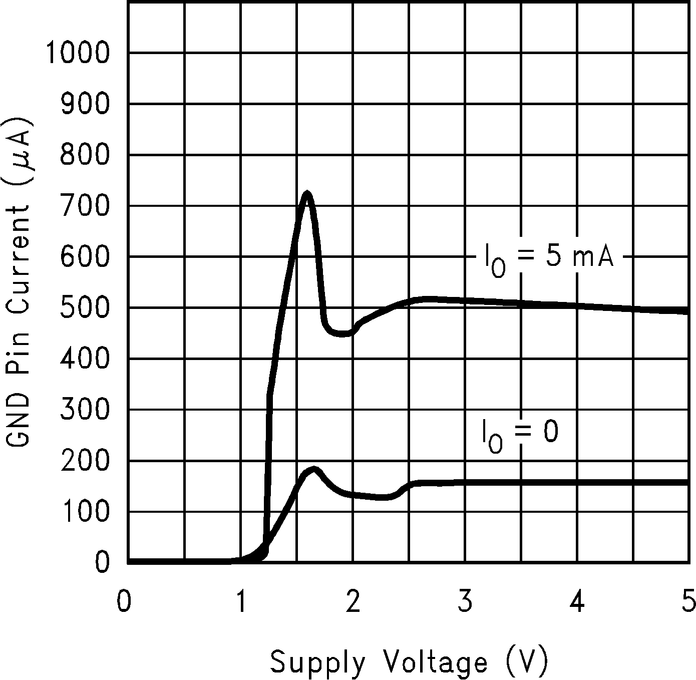 Figure 8. GND Pin Current
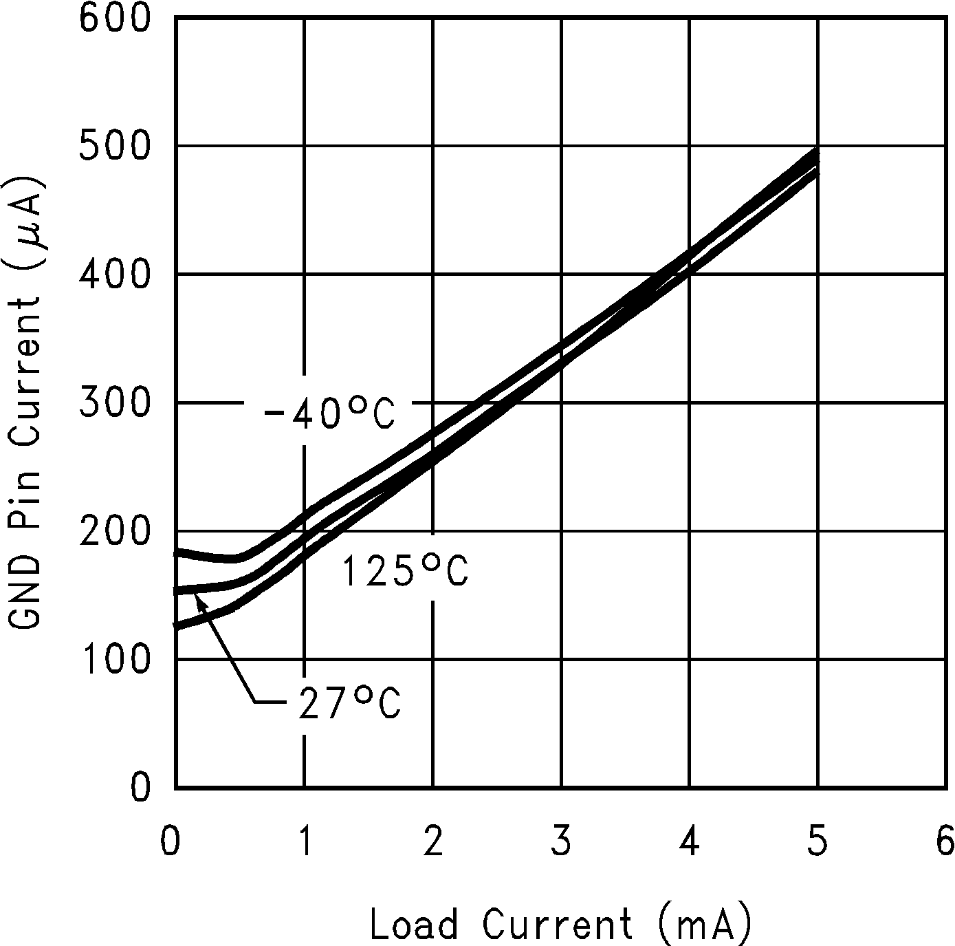 Figure 10. GND Pin Current vs Load
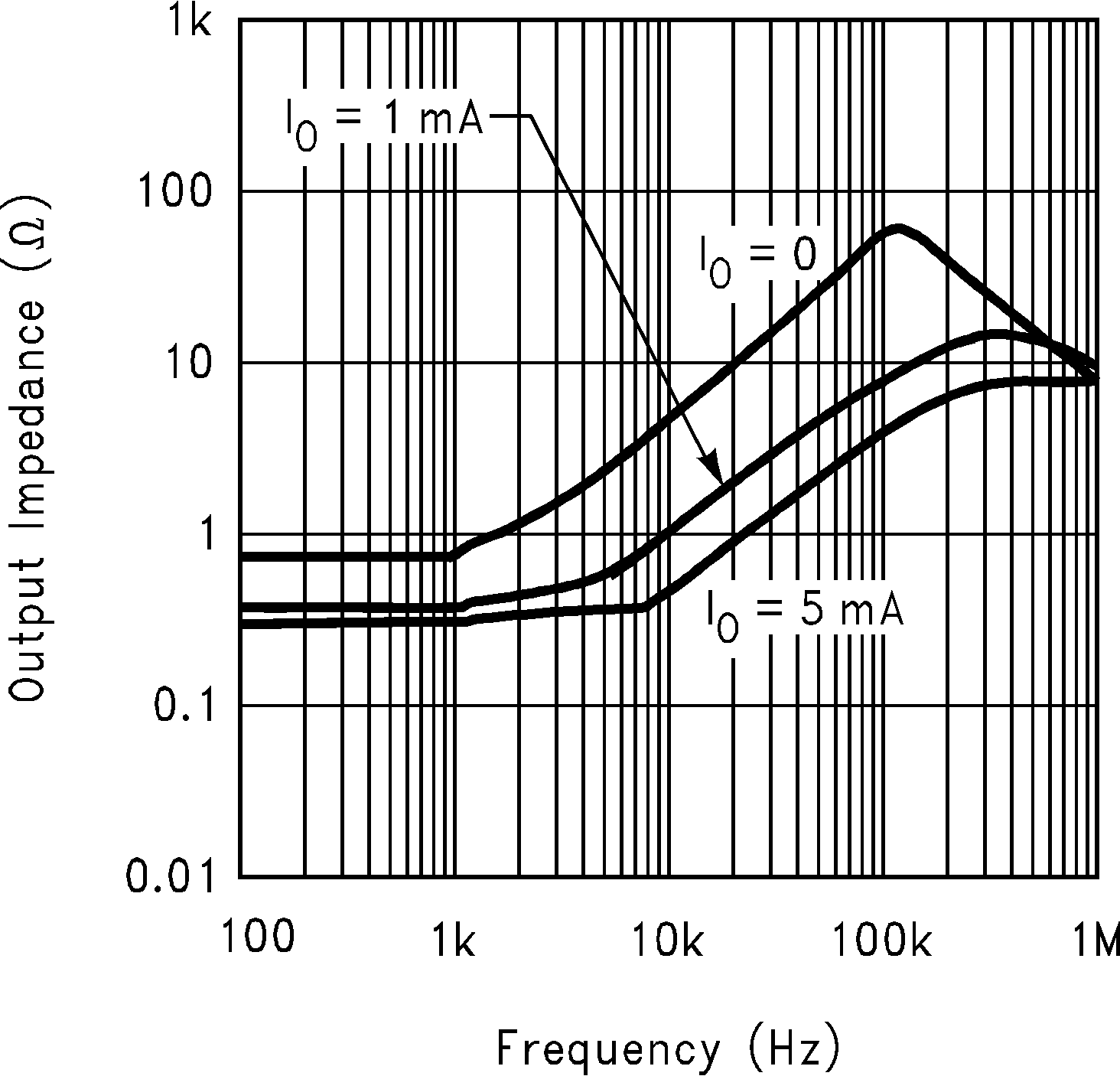 Figure 12. Output Impedance vs Frequency
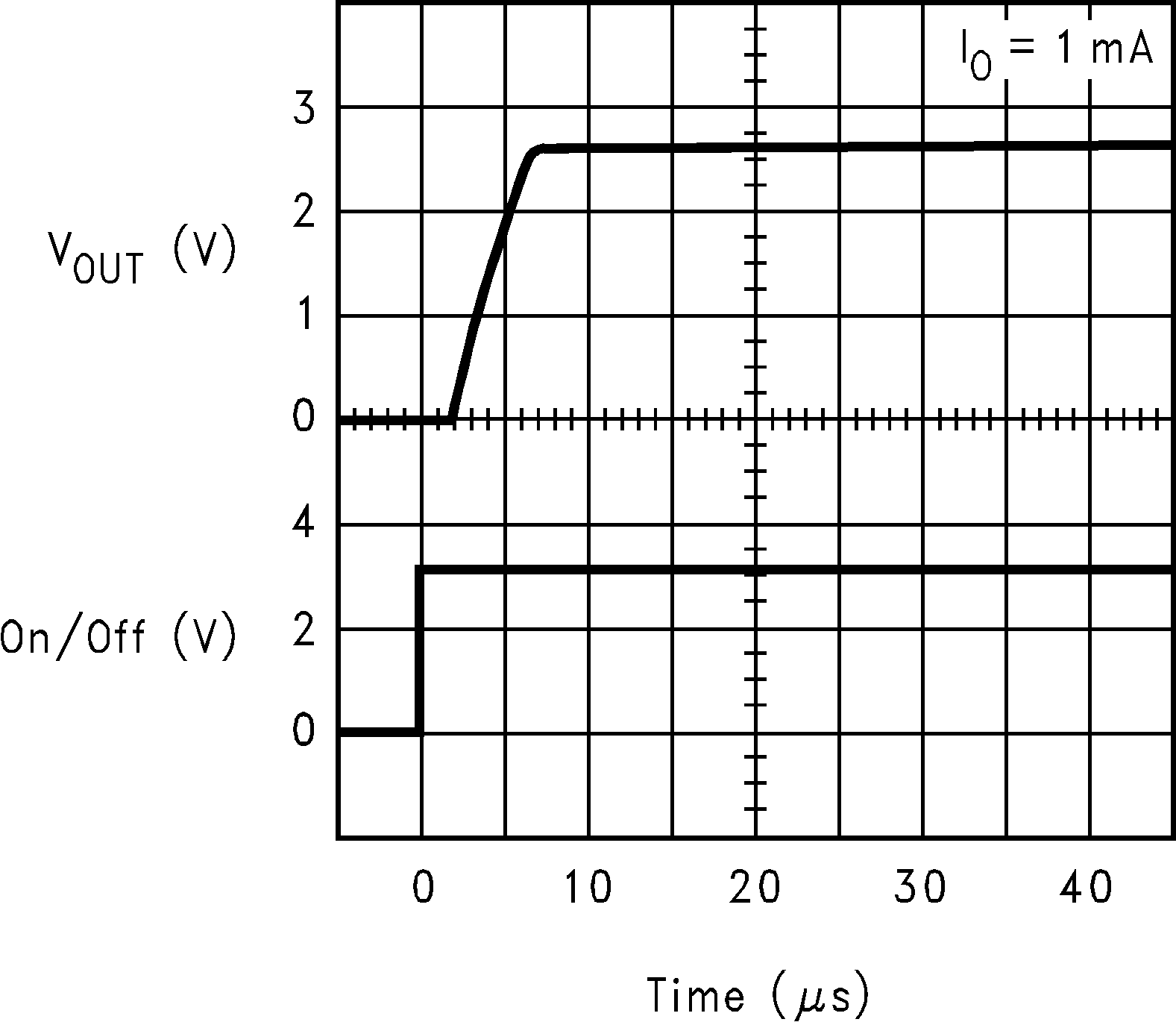 Figure 14. Enable Response
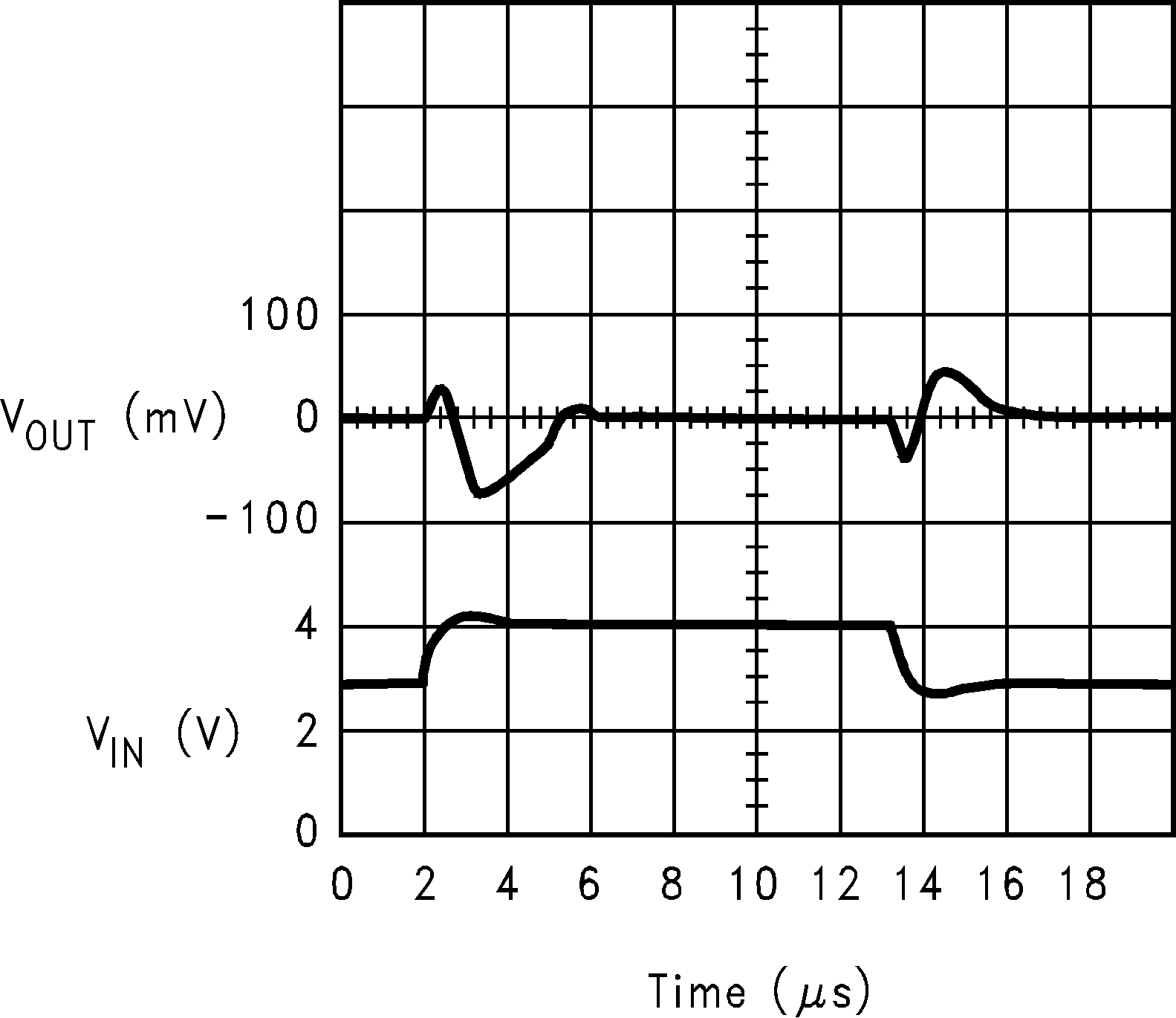 Figure 16. Line Step Response
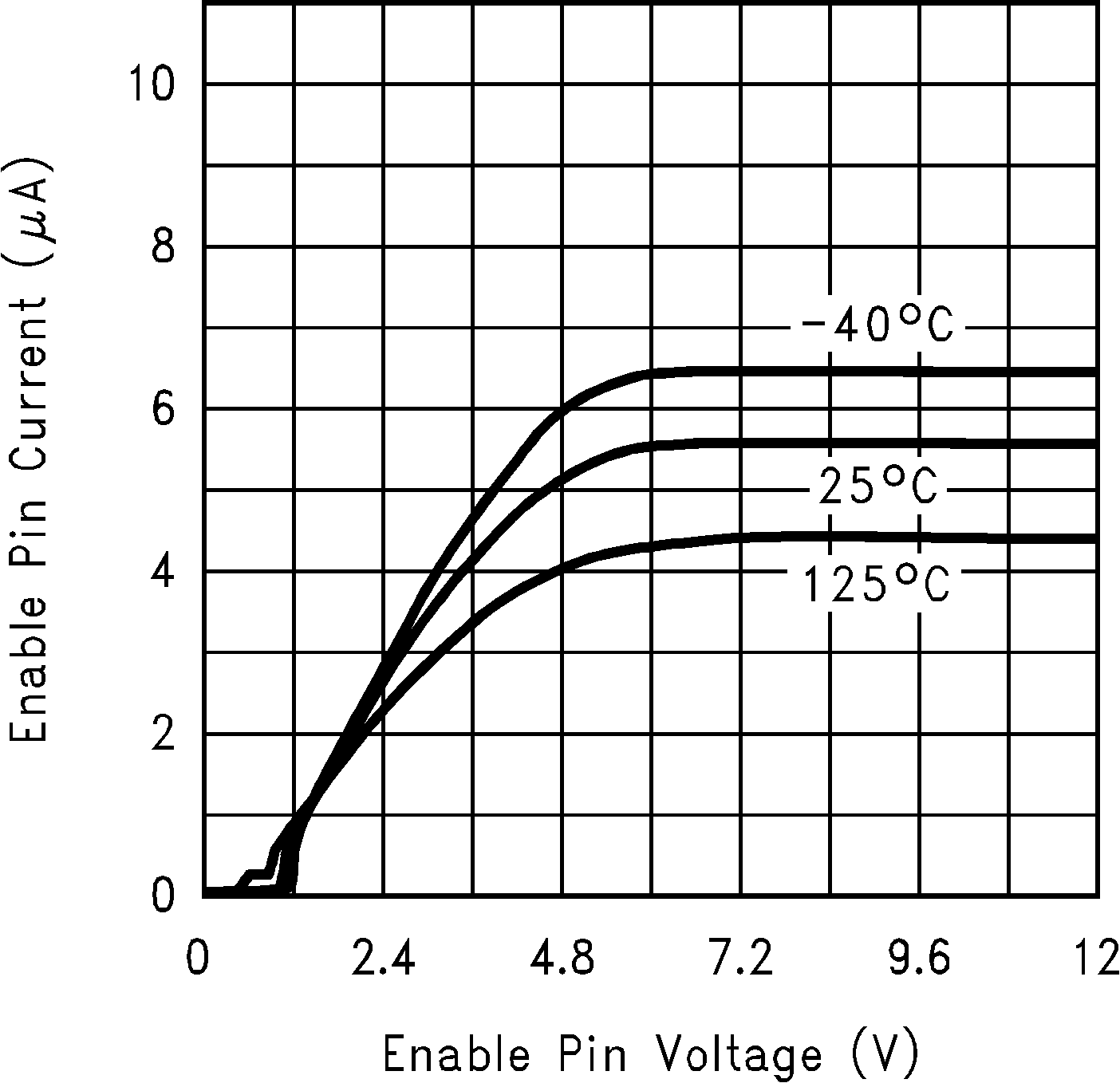 Figure 18. Enable Pin Current