SNVSA83C April 2015 – October 2017 LM43602-Q1
PRODUCTION DATA.
- 1 Features
- 2 Applications
- 3 Description
- 4 Revision History
- 5 Pin Configuration and Functions
- 6 Specifications
-
7 Detailed Description
- 7.1 Overview
- 7.2 Functional Block Diagram
- 7.3
Feature Description
- 7.3.1 Fixed Frequency Peak Current Mode Controlled Step-Down Regulator
- 7.3.2 Light Load Operation
- 7.3.3 Adjustable Output Voltage
- 7.3.4 Enable (EN)
- 7.3.5 VCC, UVLO, and BIAS
- 7.3.6 Soft Start and Voltage Tracking (SS/TRK)
- 7.3.7 Switching Frequency (RT) and Synchronization (SYNC)
- 7.3.8 Minimum ON Time, Minimum OFF Time and Frequency Foldback at Dropout Conditions
- 7.3.9 Internal Compensation and CFF
- 7.3.10 Bootstrap Voltage (BOOT)
- 7.3.11 Power Good (PGOOD)
- 7.3.12 Overcurrent and Short Circuit Protection
- 7.3.13 Thermal Shutdown
- 7.4 Device Functional Modes
-
8 Applications and Implementation
- 8.1 Application Information
- 8.2
Typical Applications
- 8.2.1 Design Requirements
- 8.2.2
Detailed Design Procedure
- 8.2.2.1 Custom Design With WEBENCH® Tools
- 8.2.2.2 Output Voltage Set-Point
- 8.2.2.3 Switching Frequency
- 8.2.2.4 Input Capacitors
- 8.2.2.5 Inductor Selection
- 8.2.2.6 Output Capacitor Selection
- 8.2.2.7 Feed-Forward Capacitor
- 8.2.2.8 Bootstrap Capacitors
- 8.2.2.9 VCC Capacitor
- 8.2.2.10 BIAS Capacitors
- 8.2.2.11 Soft-Start Capacitors
- 8.2.2.12 Undervoltage Lockout Setpoint
- 8.2.2.13 PGOOD
- 8.2.3 Application Performance Curves
- 9 Power Supply Recommendations
- 10Layout
- 11Device and Documentation Support
- 12Mechanical, Packaging, and Orderable Information
Package Options
Mechanical Data (Package|Pins)
- PWP|16
Thermal pad, mechanical data (Package|Pins)
- PWP|16
Orderable Information
7 Detailed Description
7.1 Overview
The LM43602-Q1 regulator is an easy-to-use synchronous step-down DC-DC converter that operates from 3.5-V to 36-V supply voltage. The device delivers up to 2-A DC load current with exceptional efficiency and thermal performance in a very small solution size. An extended family is available in 0.5-A, 1-A, and 3-A load options in pin-to-pin compatible packages.
The LM43602-Q1 employs fixed frequency peak current mode control with discontinuous conduction mode (DCM) and pulse frequency modulation (PFM) mode at light load to achieve high efficiency across the load range. The device is internally compensated, which reduces design time, and requires fewer external components. The switching frequency is programmable from 200 kHz to 2.2 MHz by an external resistor RT. It is default at 500 kHz without RT resistor. The LM43602-Q1 is also capable of synchronization to an external clock within the 200-kHz to 2.2-MHz frequency range. The wide switching frequency range allows the device to be optimized to fit small board space at higher frequency, or high efficient power conversion at lower frequency.
Optional features are included for more comprehensive system requirements, including power-good (PGOOD) flag, precision enable, synchronization to external clock, extendable soft-start time, and output voltage tracking. These features provide a flexible and easy to use platform for a wide range of applications. Protection features include overtemperature shutdown, VCC undervoltage lockout (UVLO), cycle-by-cycle current limit, and short-circuit protection with hiccup mode.
The family requires few external components and the pin arrangement was designed for simple, optimum PCB layout. The LM43602-Q1 device is available in the HTSSOP / PWP 16-pin leaded package.
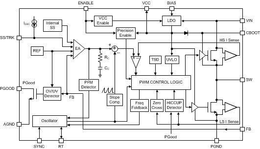
7.2 Functional Block Diagram
7.3 Feature Description
7.3.1 Fixed Frequency Peak Current Mode Controlled Step-Down Regulator
The following operating description of the LM43602-Q1 refers to the Functional Block Diagram and to the waveforms in Figure 25. The LM43602-Q1 is a step-down buck regulator with both high-side (HS) switch and low-side (LS) switch (synchronous rectifier) integrated. The LM43602-Q1 supplies a regulated output voltage by turning on the HS and LS NMOS switches with controlled ON time. During the HS switch ON time, the SW pin voltage VSW swings up to approximately VIN, and the inductor current iL increases with a linear slope (VIN – VOUT) / L. When the HS switch is turned off by the control logic, the LS switch is turned on after a anti-shoot-through dead time. Inductor current discharges through the LS switch with a slope of –VOUT / L. The control parameter of buck converters are defined as duty cycle D = tON / TSW, where tON is the HS switch ON time and TSW is the switching period. The regulator control loop maintains a constant output voltage by adjusting the duty cycle D. In an ideal buck converter, where losses are ignored, D is proportional to the output voltage and inversely proportional to the input voltage: D = VOUT / VIN.
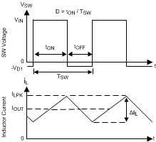 Figure 25. SW Node and Inductor Current Waveforms in Continuous Conduction Mode (CCM)
The LM43602-Q1 synchronous buck converter employs peak current mode control topology. A voltage feedback loop is used to get accurate DC voltage regulation by adjusting the peak current command based on voltage offset. The peak inductor current is sensed from the HS switch and compared to the peak current to control the ON time of the HS switch. The voltage feedback loop is internally compensated, which allows for fewer external components, makes it easy to design, and provides stable operation with almost any combination of output capacitors. The regulator operates with fixed switching frequency in Continuous Conduction Mode (CCM) and Discontinuous Conduction Mode (DCM). At very light load, the LM43602-Q1 operates in PFM to maintain high efficiency, and the switching frequency decreases with reduced load current.
7.3.2 Light Load Operation
DCM operation is employed in the LM43602-Q1 when the inductor current valley reaches zero. The LM43602-Q1 is in DCM when load current is less than half of the peak-to-peak inductor current ripple in CCM. In DCM, the LS switch is turned off when the inductor current reaches zero. Switching loss is reduced by turning off the LS FET at zero current and the conduction loss is lowered by not allowing negative current conduction. Power conversion efficiency is higher in DCM than CCM under the same conditions.
In DCM, the HS switch ON time reduces with lower load current. When either the minimum HS switch ON time (tON-MIN) or the minimum peak inductor current (IPEAK-MIN) is reached, the switching frequency decreases to maintain regulation. At this point, the LM43602-Q1 operates in PFM. In PFM, switching frequency is decreased by the control loop when load current reduces to maintain output voltage regulation. Switching loss is further reduced in PFM operation due to less frequent switching actions.
In PFM operation, a small positive DC offset is required at the output voltage to activate the PFM detector. The lower the frequency in PFM, the more DC offset is needed at VOUT. Please refer to the Typical Characteristics for typical DC offset at very light load. If the DC offset on VOUT is not acceptable for a given application, a static load at output is recommended to reduce or eliminate the offset. Lowering values of the feedback divider RFBT and RFBB can also serve as a static load. In conditions with low VIN and/or high frequency, the LM43602-Q1 may not enter PFM mode if the output voltage cannot be charged up to provide the trigger to activate the PFM detector. Once the LM43602-Q1 is operating in PFM mode at higher VIN, it remains in PFM operation when VIN is reduced
7.3.3 Adjustable Output Voltage
The voltage regulation loop in the LM43602-Q1 regulates output voltage by maintaining the voltage on FB pin (VFB) to be the same as the internal REF voltage (VREF). A resistor divider pair is needed to program the ratio from output voltage VOUT to VFB. The resistor divider is connected from the VOUT of the LM43602-Q1 to ground with the mid-point connecting to the FB pin.
 Figure 26. Output Voltage Setting
The voltage reference system produces a precise voltage reference over temperature. The internal REF voltage is 1.015 V typically. To program the output voltage of the LM43602-Q1 to be a certain value VOUT, RFBB can be calculated with a selected RFBT by

The choice of the RFBT depends on the application. RFBT in the range from 10 kΩ to 100 kΩ is recommended for most applications. A lower RFBT value can be used if static loading is desired to reduce VOUT offset in PFM operation. Lower RFBT reduces efficiency at very light load. Less static current goes through a larger RFBT and might be more desirable when light load efficiency is critical. But RFBT larger than 1 MΩ is not recommended because it makes the feedback path more susceptible to noise. Larger RFBT value requires more carefully designed feedback path on the PCB. The tolerance and temperature variation of the resistor dividers affect the output voltage regulation. It is recommended to use divider resistors with 1% tolerance or better and temperature coefficient of 100 ppm or lower.
If the resistor divider is not connected properly, output voltage cannot be regulated because the feedback loop is broken. If the FB pin is shorted to ground, the output voltage is driven close to VIN because the regulator sees very low voltage on the FB pin and tries to regulator it up. The load connected to the output could be damaged under such a condition. Do not short FB pin to ground when the LM43602-Q1 is enabled. It is important to route the feedback trace away from the noisy area of the PCB. For more layout recommendations, refer to the Layout section.
7.3.4 Enable (EN)
Voltage on the EN pin (VEN) controls the ON or OFF operation of the LM43602-Q1. Applying a voltage less than 0.4 V to the EN input shuts down the operation of the LM43602-Q1. In shutdown mode the quiescent current drops to typically 1.2 µA at VIN = 12 V.
The internal LDO output voltage VCC is turned on when VEN is higher than 1.2 V. Switching action and output regulation are enabled when VEN is greater than 2.1 V (typical). The LM43602-Q1 supplies regulated output voltage when enabled and output current up to 2 A.
The EN pin is an input and cannot be open circuit or floating. The simplest way to enable the operation of the LM43602-Q1 is to connect the EN pin to VIN pins directly. This allows self-start-up when VIN is within the operation range.
Many applications benefit from the employment of an enable divider RENT and RENB in Figure 27 to establish a precision system UVLO level for the stage. System UVLO can be used for supplies operating from utility power as well as battery power. It can be used for sequencing, ensuring reliable operation, or supply protection, such as a battery. An external logic signal can also be used to drive EN input for system sequencing and protection.
 Figure 27. System UVLO by Enable Dividers
7.3.5 VCC, UVLO, and BIAS
The LM43602-Q1 integrates an internal LDO to generate VCC for control circuitry and MOSFET drivers. The nominal voltage for VCC is 3.2 V. The VCC pin is the output of the LDO must be properly bypassed. A high-quality ceramic capacitor with 2.2-µF to 10-µF capacitance and 6.3 V or higher rated voltage should be placed as close as possible to VCC and grounded to the exposed PAD and ground pins. The VCC output pin must not be loaded, left floating, or shorted to ground during operation. Shorting VCC to ground during operation may cause damage to the LM43602-Q1.
Undervoltage lockout (UVLO) prevents the LM43602-Q1 from operating until the VCC voltage exceeds 3.15 V (typical). The VCC UVLO threshold has 575 mV of hysteresis (typically) to prevent undesired shuting down due to temporary VIN droops.
The internal LDO has two inputs: primary from VIN and secondary from BIAS input. The BIAS input powers the LDO when VBIAS is higher than the change-over threshold. Power loss of an LDO is calculated by ILDO × (VIN-LDO – VOUT-LDO). The higher the difference between the input and output voltages of the LDO, the more power loss occur to supply the same output current. The BIAS input is designed to reduce the difference of the input and output voltages of the LDO to reduce power loss and improve LM43602-Q1 efficiency, especially at light load. TI recommends tying the BIAS pin to VOUT when VOUT ≥ 3.3 V. The BIAS pin must be grounded in applications with VOUT less than 3.3 V. BIAS input can also come from an external voltage source, if available, to reduce power loss. When used, a 1-µF to 10-µF high-quality ceramic capacitor is recommended to bypass the BIAS pin to ground.
7.3.6 Soft Start and Voltage Tracking (SS/TRK)
The LM43602-Q1 has a flexible and easy to use start-up rate control pin: SS/TRK. Soft-start feature is to prevent inrush current impacting the LM43602-Q1 and its supply when power is first applied. Soft-start is achieved by slowly ramping up the target regulation voltage when the device is first enabled or powered up.
The simplest way to use the part is to leave the SS/TRK pin open circuit or floating. The LM43602-Q1 employs the internal soft-start control ramp and start up to the regulated output voltage in 4.1 ms typically.
In applications with a large amount of output capacitors, or higher VOUT, or other special requirements the soft-start time can be extended by connecting an external capacitor CSS from SS/TRK pin to AGND. Extended soft-start time further reduces the supply current needed to charge up output capacitors and supply any output loading. An internal current source (ISSC = 2.2 µA) charges CSS and generates a ramp from 0 V to VFB to control the ramp-up rate of the output voltage. For a desired soft start time tSS, the capacitance for CSS can be found by

The LM43602-Q1 is capable of start up into prebiased output conditions. When the inductor current reaches zero, the LS switch is turned off to avoid negative current conduction. This operation mode is also called diode emulation mode. It is built-in by the DCM operation in light loads. With prebiased output voltage, the LM43602-Q1 waits until the soft-start ramp allows regulation above the prebiased voltage and then follows the soft-start ramp to regulation level.
When an external voltage ramp is applied to the SS/TRK pin, the LM43602-Q1 FB voltage follows the ramp if the ramp magnitude is lower than the internal soft-start ramp. A resistor divider pair can be used on the external control ramp to the SS/TRK pin to program the tracking rate of the output voltage. The final voltage seen by the SS/TRK pin should not fall below 1.2 V to avoid abnormal operation.
 Figure 28. Soft Start Tracking External Ramp
VOUT tracked to external voltage ramps has options of ramping up slower or faster than the internal voltage ramp. VFB always follows the lower potential of the internal voltage ramp and the voltage on the SS/TRK pin. Figure 29 shows the case when VOUT ramps slower than the internal ramp, while Figure 30 shows when VOUT ramps faster than the internal ramp. Faster start-up time may result in inductor current tripping current protection during start-up. Use with special care.
7.3.7 Switching Frequency (RT) and Synchronization (SYNC)
The switching frequency of the LM43602-Q1 can be programmed by the impedance RT from the RT pin to ground. The frequency is inversely proportional to the RT resistance. The RT pin can be left floating and the LM43602-Q1 operates at 500-kHz default switching frequency. The RT pin is not designed to be shorted to ground. For a desired frequency, typical RT resistance can be found by Equation 3. Table 1 gives typical RT values with a given FS.
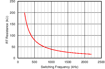 Figure 31. RT vs Frequency Curve
Table 1. Typical Frequency Setting RT Resistance
| FS (kHz) | RT (kΩ) |
|---|---|
| 200 | 200 |
| 350 | 115 |
| 500 | 78.7 |
| 750 | 53.6 |
| 1000 | 39.2 |
| 1500 | 26.1 |
| 2000 | 19.6 |
| 2200 | 17.8 |
The LM43602-Q1 switching action can also be synchronized to an external clock from 200 kHz to 2.2 MHz. Connect an external clock to the SYNC pin, with proper high-speed termination, to avoid ringing. Ground the SYNC pin if not used.
 Figure 32. Frequency Synchronization
The recommendations for the external clock include: high level no lower than 2 V, low level no higher than 0.4 V, duty cycle between 10% and 90% and both positive and negative pulse width no shorter than 80 ns. When the external clock fails at logic high or low, the LM43602-Q1 switches at the frequency programmed by the RT resistor after a time-out period. It is recommended to connect a resistor RT to the RT pin such that the internal oscillator frequency is the same as the target clock frequency when the LM43602-Q1 is synchronized to an external clock. This allows the regulator to continue operating at approximately the same switching frequency if the external clock fails.
The choice of switching frequency is usually a compromise between conversion efficiency and the size of the circuit. Lower switching frequency implies reduced switching losses (including gate charge losses, switch transition losses, etc.) and usually results in higher overall efficiency. However, higher switching frequency allows use of smaller LC output filters and hence a more compact design. Lower inductance also helps transient response (higher large signal slew rate of inductor current), and reduces the DCR loss. The optimal switching frequency is usually a trade-off in a given application and thus needs to be determined on a case-by-case basis. It is related to the input voltage, output voltage, most frequent load current level(s), external component choices, and circuit size requirement. The choice of switching frequency may also be limited if an operating condition triggers TON-MIN or TOFF-MIN.
7.3.8 Minimum ON Time, Minimum OFF Time and Frequency Foldback at Dropout Conditions
Minimum ON time, TON-MIN, is the smallest duration of time that the HS switch can be on. TON-MIN value is typically 125 ns in the LM43602-Q1. Minimum OFF time, TOFF-MIN, is the smallest duration that the HS switch can be off. TOFF-MIN is typically 200 ns in the LM43602-Q1.
In CCM operation, TON-MIN and TOFF-MIN limits the voltage conversion range given a selected switching frequency. The minimum duty cycle allowed is
And the maximum duty cycle allowed is
Given fixed TON-MIN and TOFF-MIN, the higher the switching frequency the narrower the range of the allowed duty cycle. In the LM43602-Q1, frequency foldback scheme is employed to extend the maximum duty cycle when TOFF-MIN is reached. The switching frequency decreases once longer duty cycle is needed under low VIN conditions. The switching frequency can be decreased to approximately 1/10 of the programmed frequency by RT or the synchronization clock. Such wide range of frequency foldback allows the LM43602-Q1 output voltage stays in regulation with much lower supply voltage VIN. This leads to a lower effective dropout voltage. Refer to Typical Characteristics for more details.
Given a output voltage, the choice of the switching frequency affects the allowed input voltage range, solution size, and efficiency. The maximum operatable supply voltage can be found by Equation 6:
At lower supply voltage, the switching frequency decreases once TOFF-MIN is tripped. The minimum VIN without frequency foldback can be approximated by Equation 7:
Taking considerations of power losses in the system with heavy load operation, VIN-MIN is higher than the result calculated in Equation 7 . With frequency foldback, VIN-MIN is lowered by decreased FS.
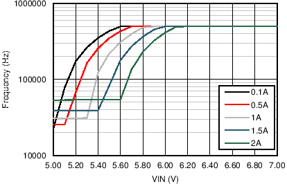 Figure 33. VOUT = 5 V Fs = 500 kHz
Frequency Foldback at Dropout
7.3.9 Internal Compensation and CFF
The LM43602-Q1 is internally compensated with RC = 400 kΩ and CC = 50 pF as shown in Functional Block Diagram. The internal compensation is designed such that the loop response is stable over the entire operating frequency and output voltage range. Depending on the output voltage, the compensation loop phase margin can be low with all ceramic capacitors. TI recommends an external feed-forward capacitor, CFF, be placed in parallel with the top resistor divider RFBT for optimum transient performance.
 Figure 34. Feed-Forward Capacitor for Loop Compensation
The feed-forward capacitor CFF in parallel with RFBT places an additional zero before the crossover frequency of the control loop to boost phase margin. The zero frequency can be found by Equation 8:
An additional pole is also introduced with CFF at the frequency of:
Select the CFF so that the bandwidth of the control loop without the CFF is centered between fZ-CFF and fP-CFF. The zero fZ-CFF adds phase boost at the crossover frequency and improves transient response. The pole fP-CFF helps maintaining proper gain margin at frequency beyond the crossover.
Designs with different combinations of output capacitors need different CFF. Different types of capacitors have different equivalent series resistance (ESR). Ceramic capacitors have the smallest ESR and need the most CFF. Electrolytic capacitors have much larger ESR and the ESR zero frequency
would be low enough to boost the phase up around the crossover frequency. Designs using mostly electrolytic capacitors at the output may not need any CFF.
The CFF creates a time constant with RFBT that couples in the attenuated output voltage ripple to the FB node. If the CFF value is too large, it can couple too much ripple to the FB and affect VOUT regulation. It could also couple too much transient voltage deviation and falsely trip PGOOD thresholds. Therefore, calculate CFF based on output capacitors used in the system. At cold temperatures, the value of CFF might change based on the tolerance of the chosen component. This may reduce its impedance and ease noise coupling on the FB node. To avoid this, more capacitance can be added to the output or the value of CFF can be reduced. Refer to the Detailed Design Procedure for the calculation of CFF.
7.3.10 Bootstrap Voltage (BOOT)
The driver of the HS switch requires a bias voltage higher than VIN when the HS switch is ON. The capacitor connected between CBOOT and SW pins works as a charge pump to boost voltage on the CBOOT pin to (VSW + VCC). The boot diode is integrated on the LM43602-Q1 die to minimize bill of material (BOM). A synchronous switch is also integrated in parallel with the boot diode to reduce voltage drop on CBOOT. A high-quality ceramic 0.47-µF, 6.3-V or higher capacitor is recommended for CBOOT.
7.3.11 Power Good (PGOOD)
The LM43602-Q1 has a built-in power-good flag shown on PGOOD pin to indicate whether the output voltage is within its regulation level. The PGOOD signal can be used for start-up sequencing of multiple rails or fault protection. The PGOOD pin is an open-drain output that requires a pullup resistor to an appropriate DC voltage. Voltage detected by the PGOOD pin must never exceed 12 V. A resistor divider pair can be used to divide voltage down from a higher potential. A typical range of pullup resistor value is 10 kΩ to 100 kΩ.
When the FB voltage is within the power-good band, +4% above and –7% below the internal reference VREF typically, the PGOOD switch will be turned off, and the PGOOD voltage will be pulled up to the voltage level defined by the pullup resistor or divider. When the FB voltage is outside of the tolerance band, +10% above or -13% below VREF typically, the PGOOD switch will be turned on, and the PGOOD pin voltage will be pulled low to indicate power bad. Both rising and falling edges of the power-good flag have a built-in 220 µs (typical) deglitch delay.
7.3.12 Overcurrent and Short Circuit Protection
The LM43602-Q1 is protected from overcurrent conditions by cycle-by-cycle current limiting on both peak and valley of the inductor current. Hiccup mode is activated if a fault condition persists to prevent overheating.
High-side MOSFET overcurrent protection is implemented by the nature of the peak current mode control. The HS switch current is sensed when the HS is turned on after a set blanking time. The HS switch current is compared to the output of the error amplifier (EA) minus slope compensation every switching cycle. Refer to Functional Block Diagram for more details. The peak current of the HS switch is limited by the maximum EA output voltage minus the slope compensation at every switching cycle. The slope compensation magnitude at the peak current is proportional to the duty cycle.
When the LS switch is turned on, the current going through it is also sensed and monitored. The LS switch is not turned OFF at the end of a switching cycle if its current is above the LS current limit ILS-LIMIT. The LS switch is kept ON so that inductor current keeps ramping down, until the inductor current ramps below the LS current limit. Then the LS switch is then turned OFF, and the HS switch turned on, after a dead time. If the current of the LS switch is higher than the LS current limit for 32 consecutive cycles and the power-good flag is low, hiccup current protection mode is activated. In hiccup mode, the regulator is shut down and kept off for 5.5 ms typically before the LM43602-Q1 tries to start again. If overcurrent or short-circuit fault condition still exists, hiccup repeats until the fault condition is removed. Hiccup mode reduces power dissipation under severe overcurrent conditions, prevents over heating and potential damage to the device.
Hiccup is only activated when power-good flag is low. Under non-severe overcurrent conditions when VOUT has not fallen outside of the PGOOD tolerance band, the LM43602-Q1 reduces the switching frequency and keeps the inductor current valley clamped at the LS current limit level. This operation mode allows slight overcurrent operation during load transients without tripping hiccup. If power-good flag becomes low, hiccup operation starts after LS current limit is tripped 32 consecutive cycles.
7.3.13 Thermal Shutdown
Thermal shutdown is a built-in self protection to limit junction temperature and prevent damages due to overheating. Thermal shutdown turns off the device when the junction temperature exceeds 160°C typically to prevent further power dissipation and temperature rise. Junction temperature reduces after thermal shutdown. The LM43602-Q1 attempts to restart when the junction temperature drops to 150°C.
7.4 Device Functional Modes
7.4.1 Shutdown Mode
The EN pin provides electrical ON and OFF control for the LM43602-Q1. When VEN is below 0.4 V, the device is in shutdown mode. Both the internal LDO and the switching regulator are off. In shutdown mode the quiescent current drops to 2.3 µA typically with VIN = 24 V. The LM43602-Q1 also employs undervoltage lockout protection. If VCC voltage is below the UVLO level, the output of the regulator is turned off.
7.4.2 Standby Mode
The internal LDO has a lower enable threshold than the regulator. When VEN is above 1.2 V and below the precision enable falling threshold (1.8 V typically), the internal LDO regulates the VCC voltage at 3.2 V. The precision enable circuitry is turned on once VCC is above the UVLO threshold. The switching action and voltage regulation are not enabled unless VEN rises above the precision enable threshold (2.1 V typically).
7.4.3 Active Mode
The LM43602-Q1 is in active mode when VEN is above the precision enable threshold and VCC is above its UVLO level. The simplest way to enable the LM43602-Q1 is to connect the EN pin to VIN. This allows self start-up when the input voltage is in the operation range: 3.5 V to 36 V. Refer to Enable (EN) and VCC, UVLO, and BIAS for details on setting these operating levels.
In active mode, depending on the load current, the LM43602-Q1 is in one of four modes:
- Continuous conduction mode (CCM) with fixed switching frequency when load current is above half of the peak-to-peak inductor current ripple;
- Discontinuous conduction mode (DCM) with fixed switching frequency when load current is lower than half of the peak-to-peak inductor current ripple in CCM operation;
- Pulse frequency modulation (PFM) when switching frequency is decreased at very light load;
- Foldback mode when switching frequency is decreased to maintain output regulation at lower supply voltage VIN.
7.4.4 CCM Mode
CCM operation is employed in the LM43602-Q1 when the load current is higher than half of the peak-to-peak inductor current. In CCM operation, the frequency of operation is fixed unless the the minimum HS switch ON-time (TON_MIN) or OFF-time (TOFF_MIN) is exceeded. Output voltage ripple is at a minimum in this mode and the maximum output current of 2 A can be supplied by the LM43602-Q1.
7.4.5 Light Load Operation
When the load current is lower than half of the peak-to-peak inductor current in CCM, the LM43602-Q1 operates in DCM, also known as diode emulation mode (DEM). In DCM operation, the LS FET is turned off when the inductor current drops to 0 A to improve efficiency. Both switching losses and conduction losses are reduced in DCM, comparing to forced PWM operation at light load.
At even lighter current loads, PFM is activated to maintain high efficiency operation. When the HS switch ON time reduces to TON_MIN or peak inductor current reduces to its minimum IPEAK-MIN, the switching frequency reduces to maintain proper regulation. Efficiency is greatly improved by reducing switching and gate drive losses.
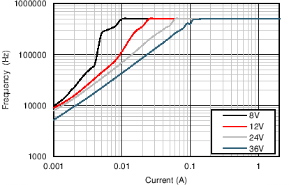 Figure 35. VOUT = 5 V Fs = 500 kHz
Pulse Frequency Mode Operation
7.4.6 Self-Bias Mode
For highest efficiency of operation, TI recommends that the BIAS pin be connected directly to VOUT when VOUT ≥ 3.3 V. In this self-bias mode of operation, the difference between the input and output voltages of the internal LDO are reduced and, therefore, the total efficiency is improved. These efficiency gains are more evident during light load operation. During this mode of operation, the LM43602-Q1 operates with a minimum quiescent current of 27 µA (typical). Refer to VCC, UVLO, and BIAS for more details.