SNVSA82C April 2015 – October 2017 LM43603-Q1
PRODUCTION DATA.
- 1 Features
- 2 Applications
- 3 Description
- 4 Revision History
- 5 Pin Configuration and Functions
- 6 Specifications
-
7 Detailed Description
- 7.1 Overview
- 7.2 Functional Block Diagram
- 7.3
Feature Description
- 7.3.1 Fixed Frequency Peak Current Mode Controlled Step-Down Regulator
- 7.3.2 Light Load Operation
- 7.3.3 Adjustable Output Voltage
- 7.3.4 Enable (EN)
- 7.3.5 VCC, UVLO, and BIAS
- 7.3.6 Soft-Start and Voltage Tracking (SS/TRK)
- 7.3.7 Switching Frequency (RT) and Synchronization (SYNC)
- 7.3.8 Minimum ON Time, Minimum OFF Time and Frequency Foldback at Dropout Conditions
- 7.3.9 Internal Compensation and CFF
- 7.3.10 Bootstrap Voltage (BOOT)
- 7.3.11 Power Good (PGOOD)
- 7.3.12 Overcurrent and Short-Circuit Protection
- 7.3.13 Thermal Shutdown
- 7.4 Device Functional Modes
-
8 Applications and Implementation
- 8.1 Application Information
- 8.2
Typical Applications
- 8.2.1 Design Requirements
- 8.2.2
Detailed Design Procedure
- 8.2.2.1 Custom Design With WEBENCH® Tools
- 8.2.2.2 Output Voltage Setpoint
- 8.2.2.3 Switching Frequency
- 8.2.2.4 Input Capacitors
- 8.2.2.5 Inductor Selection
- 8.2.2.6 Output Capacitor Selection
- 8.2.2.7 Feed-Forward Capacitor
- 8.2.2.8 Bootstrap Capacitors
- 8.2.2.9 VCC Capacitor
- 8.2.2.10 BIAS Capacitors
- 8.2.2.11 Soft-Start Capacitors
- 8.2.2.12 Undervoltage Lockout Setpoint
- 8.2.2.13 PGOOD
- 8.2.3 Application Performance Curves
- 9 Power Supply Recommendations
- 10Layout
- 11Device and Documentation Support
- 12Mechanical, Packaging, and Orderable Information
Package Options
Mechanical Data (Package|Pins)
- PWP|16
Thermal pad, mechanical data (Package|Pins)
- PWP|16
Orderable Information
8 Applications and Implementation
NOTE
Information in the following applications sections is not part of the TI component specification, and TI does not warrant its accuracy or completeness. TI’s customers are responsible for determining suitability of components for their purposes. Customers should validate and test their design implementation to confirm system functionality.
8.1 Application Information
The LM43603-Q1 is a step-down DC-DC regulator. It is typically used to convert a higher DC voltage to a lower DC voltage with a maximum output current of 3 A. The following design procedure can be used to select components for the LM43603-Q1.
8.2 Typical Applications
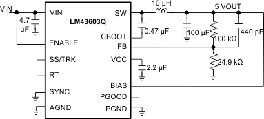
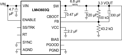
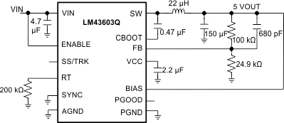
The LM43603-Q1 only requires a few external components to convert from a wide voltage range supply to a fixed output voltage. Figure 46 shows a basic schematic when BIAS is connected to VOUT and this is recommended for VOUT ≥ 3.3 V. For VOUT < 3.3 V, connect BIAS to ground, as shown in Figure 47.
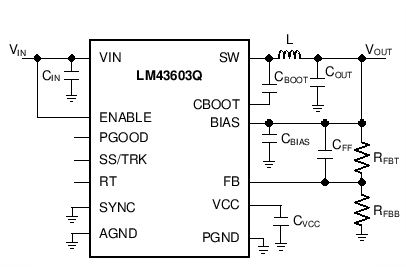 Figure 46. LM43603-Q1 Basic Schematic for VOUT ≥ 3.3 V, tie BIAS to VOUT
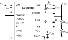 Figure 47. LM43603-Q1 Basic Schematic for VOUT < 3.3 V, tie BIAS to Ground
The LM43603-Q1 also integrates a full list of optional features to aid system design requirements such as precision enable, VCC UVLO, programmable soft start, output voltage tracking, programmable switching frequency, clock synchronization and power-good indication. Each application can select the features for a more comprehensive design. A schematic with all features utilized is shown in Figure 48.
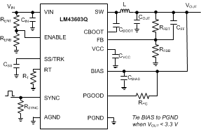 Figure 48. LM43603-Q1 Schematic with All Features
The external components must fulfill the needs of the application, as well as the stability criteria of the device control loop. The LM43603-Q1 is optimized to work within a range of external components. The inductance and capacitance of the LC output filter must considered in conjunction, creating a double pole, responsible for the corner frequency of the converter. Table 2 can be used to simplify the output filter component selection.
Table 2. L, COUT and CFF Typical Values
| FS (kHz) | VOUT (V) | L (µH)(2) | COUT (µF) (1) | CFF (pF) (3)(4) | RT (kΩ) | RFBB (kΩ) (3)(4) |
|---|---|---|---|---|---|---|
| 200 | 1 | 4.8 | 600 | none | 200 | 100 |
| 500 | 1 | 2.2 | 400 | none | 80.6 or open | 100 |
| 1000 | 1 | 1 | 250 | none | 39.2 | 100 |
| 2200 | 1 | 0.47 | 150 | none | 17.8 | 100 |
| 200 | 3.3 | 15 | 300 | 470 | 200 | 43.2 |
| 500 | 3.3 | 4.7 | 150 | 330 | 80.6 or open | 43.2 |
| 1000 | 3.3 | 3.3 | 100 | 220 | 39.2 | 43.2 |
| 2200 | 3.3 | 1 | 50 | 180 | 17.8 | 43.2 |
| 200 | 5 | 18 | 200 | 680 | 200 | 24.9 |
| 500 | 5 | 6.8 | 120 | 440 | 80.6 or open | 24.9 |
| 1000 | 5 | 3.3 | 100 | 330 | 39.2 | 24.9 |
| 2200 | 5 | 1.5 | 50 | 220 | 17.8 | 24.9 |
| 200 | 12 | 33 | 100 | See(5) | 200 | 9.09 |
| 500 | 12 | 15 | 50 | 680 | 80.6 or open | 9.09 |
| 1000 | 12 | 6.8 | 44 | 560 | 39.2 | 9.09 |
| 200 | 24 | 44 | 47 | See(5) | 200 | 4.32 |
| 500 | 24 | 18 | 47 | See(5) | 80.6 or open | 4.32 |
| 1000 | 24 | 10 | 33 | See(5) | 39.2 | 4.32 |
8.2.1 Design Requirements
Detailed design procedure is described based on a design example. For this design example, use the parameters listed in Table 3 as the input parameters.
Table 3. Design Example Parameters
| DESIGN PARAMETER | VALUE |
|---|---|
| Input voltage VIN | 12 V typical, range from 3.5 V to 36 V |
| Output voltage VOUT | 3.3 V |
| Input ripple voltage | 400 mV |
| Output ripple voltage | 30 mV |
| Output current rating | 3 A |
| Operating frequency | 500 kHz |
| Soft-start time | 10 ms |
8.2.2 Detailed Design Procedure
8.2.2.1 Custom Design With WEBENCH® Tools
Click here to create a custom design using the LM43603-Q1 device with the WEBENCH® Power Designer.
- Start by entering the input voltage (VIN), output voltage (VOUT), and output current (IOUT) requirements.
- Optimize the design for key parameters such as efficiency, footprint, and cost using the optimizer dial.
- Compare the generated design with other possible solutions from Texas Instruments.
The WEBENCH Power Designer provides a customized schematic along with a list of materials with real-time pricing and component availability.
In most cases, these actions are available:
- Run electrical simulations to see important waveforms and circuit performance
- Run thermal simulations to understand board thermal performance
- Export customized schematic and layout into popular CAD formats
- Print PDF reports for the design, and share the design with colleagues
Get more information about WEBENCH tools at www.ti.com/WEBENCH.
8.2.2.2 Output Voltage Setpoint
The output voltage of the LM43603-Q1 device is externally adjustable using a resistor divider network. The divider network is comprised of top feedback resistor RFBT and bottom feedback resistor RFBB. Equation 11 is used to determine the output voltage of the converter:

Choose the value of the RFBT to be 100 kΩ to minimize quiescent current to improve light load efficiency in this application. With the desired output voltage set to be 3.3 V and the VFB = 1.015 V, the RFBB value can then be calculated using Equation 11. The formula yields a value of 43.478 kΩ. Choose the closest available value of 43.2 kΩ for the RFBB. See Adjustable Output Voltage for more details.
8.2.2.3 Switching Frequency
The default switching frequency of the LM43603-Q1 device is set at 500 kHz when RT pin is open circuit. The switching frequency is selected to be 500 kHz in this application for one less passive components. If other frequency is desired, use Equation 12 to calculate the required value for RT.
For 500 kHz, the calculated RT is 79.8 kΩ and standard value 80.6 kΩ can also be used to set the switching frequency at 500 kHz.
8.2.2.4 Input Capacitors
The LM43603-Q1 device requires high frequency input decoupling capacitor(s) and a bulk input capacitor, depending on the application. The typical recommended value for the high frequency decoupling capacitor is between 4.7 µF to 10 µF. TI recommends a high-quality ceramic type X5R or X7R with sufficiency voltage rating. The voltage rating must be greater than the maximum input voltage. To compensate the derating of ceramic capactors, TI recommends a voltage rating of twice the maximum input voltage. Additionally, some bulk capacitance can be required, especially if the LM43603-Q1 circuit is not located within approximately 5 cm from the input voltage source. This capacitor is used to provide damping to the voltage spiking due to the lead inductance of the cable or trace. The value for this capacitor is not critical but must be rated to handle the maximum input voltage including ripple. For this design, a 10-µF, X7R dielectric capacitor rated for 100 V is used for the input decoupling capacitor. The ESR is approximately 3 mΩ, and the current-rating is 3 A. Include a capacitor with a value of 0.1 µF for high-frequency filtering and place it as close as possible to the device pins.
NOTE
DC Bias effect: High capacitance ceramic capacitors have a DC bias effect, which will have a strong influence on the final effective capacitance. Therefore, carefully choose the correct capacitor value. Package size and voltage rating in combination with dielectric material are responsible for differences between the rated capacitor value and the effective capacitance.
8.2.2.5 Inductor Selection
The first criterion for selecting an output inductor is the inductance itself. In most buck converters, this value is based on the desired peak-to-peak ripple current, ΔiL, that flows in the inductor along with the DC load current. As with switching frequency, the selection of the inductor is a tradeoff between size and cost. Higher inductance gives lower ripple current and hence lower output voltage ripple with the same output capacitors. Lower inductance could result in smaller, less expensive component. An inductance that gives a ripple current of 20% to 40% of the 3 A at the typical supply voltage is a good starting point. ΔiL = (1/5 to 2/5) × IOUT. The peak-to-peak inductor current ripple can be found by Equation 13 and the range of inductance can be found by Equation 14 with the typical input voltage used as VIN.


D is the duty cycle of the converter where in a buck converter case it can be approximated as D = VOUT / VIN, assuming no loss power conversion. By calculating in terms of amperes, volts, and megahertz, the inductance value will come out in micro Henries. The inductor ripple current ratio is defined by:

The second criterion is inductor saturation current rating. The inductor must be rated to handle the maximum load current plus the ripple current:
The LM43603-Q1 has both valley current limit and peak current limit. During an instantaneous short, the peak inductor current can be high due to a momentary increase in duty cycle. The inductor current rating must be higher than the HS current limit. It is advised to select an inductor with a larger core saturation margin and preferably a softer roll off of the inductance value over load current.
In general, it is preferable to choose lower inductance in switching power supplies, because it usually corresponds to faster transient response, smaller DCR, and reduced size for more compact designs. But too low of an inductance can generate too large of an inductor current ripple such that over current protection at the full load could be falsely triggered. It also generates more conduction loss, because the RMS current is slightly higher relative that with lower current ripple at the same DC current. Larger inductor current ripple also implies larger output voltage ripple with the same output capacitors. With peak current mode control, it is not recommended to have too small of an inductor current ripple. A larger peak current ripple improves the comparator signal to noise ratio.
Once the inductance is determined, the type of inductor must be selected. Ferrite designs have very low core losses and are preferred at high switching frequencies, so design goals can concentrate on copper loss and preventing saturation. Ferrite core material saturates hard, which means that inductance collapses abruptly when the peak design current is exceeded. The ‘hard’ saturation results in an abrupt increase in inductor ripple current and consequent output voltage ripple. Do not allow the core to saturate!
For the design example, a standard 6.8 μH inductor from Würth Elektronik, Coilcraft, or Vishay can be used for the 3.3 V output with plenty of current rating margin.
8.2.2.6 Output Capacitor Selection
The device is designed to be used with a wide variety of LC filters. Use as little output capacitance as possible to keep cost and size down. Choose the output capacitor(s), COUT, with care because it directly affects the steady state output voltage ripple, loop stability and the voltage over/undershoot during load current transients.
The output voltage ripple is essentially composed of two parts. One is caused by the inductor current ripple going through the ESR of the output capacitors:
The other is caused by the inductor current ripple charging and discharging the output capacitors:
The two components in the voltage ripple are not in phase, so the actual peak-to-peak ripple is smaller than the sum of the two peaks.
Output capacitance is usually limited by transient performance specifications if the system requires tight voltage regulation with presence of large current steps and fast slew rates. When a fast large load transient happens, output capacitors provide the required charge before the inductor current can slew to the appropriate level. The initial output voltage step is equal to the load current step multiplied by the ESR. VOUT continues to droop until the control loop response increases or decreases the inductor current to supply the load. To maintain a small overshoot or undershoot during a transient, small ESR and large capacitance are desired. But these also come with higher cost and size. Thus, the motivation is to seek a fast control loop response to reduce the output voltage deviation.
For a given input and output requirement, Equation 19 gives an approximation for an absolute minimum output capacitor required:

Along with this for the same requirement, calculate the maximum ESR as per Equation 20:

where
- r = Ripple ratio of the inductor ripple current (ΔIL / IOUT)
- ΔVOUT = target output voltage undershoot
- D’ = 1 – duty cycle
- FS = switching frequency
- IOUT = load current
A general guideline for COUT range is that COUT must be larger than the minimum required output capacitance calculated by Equation 19, and smaller than 10 times the minimum required output capacitance or 1 mF. In applications with VOUT less than 3.3 V, it is critical that low ESR output capacitors are selected. This limits potential output voltage overshoots as the input voltage falls below the device normal operating range. To optimize the transient behavior a feed-forward capacitor could be added in parallel with the upper feedback resistor. For this design example, three 47-µF, 10-V, X7R ceramic capacitors are used in parallel.
8.2.2.7 Feed-Forward Capacitor
The LM43603-Q1 is internally compensated and the internal R-C values are 400 kΩ and 50 pF, respectively. Depending on the VOUT and frequency FS, if the output capacitor COUT is dominated by low ESR (ceramic types) capacitors, it could result in low phase margin. To improve the phase boost an external feedforward capacitor CFF can be added in parallel with RFBT. CFF is chosen such that phase margin is boosted at the crossover frequency without CFF. A simple estimation for the crossover frequency without CFF (fx) is shown in Equation 21, assuming COUT has very small ESR.

Equation 22 was tested for CFF:

This equation indicates that the crossover frequency is geometrically centered on the zero and pole frequencies caused by the CFF capacitor.
For designs with higher ESR, CFF is not needed when COUT has very high ESR, and CFF calculated from Equation 22 must be reduced with medium ESR. Table 2 can be used as a quick starting point.
For the application in this design example, a 470 pF COG capacitor is selected.
8.2.2.8 Bootstrap Capacitors
Every LM43603-Q1 design requires a bootstrap capacitor, CBOOT. The recommended bootstrap capacitor value is 0.47 μF and rated at 6.3 V or higher. The bootstrap capacitor is located between the SW pin and the CBOOT pin. The bootstrap capacitor must be a high-quality ceramic type with X7R or X5R grade dielectric for temperature stability.
8.2.2.9 VCC Capacitor
The VCC pin is the output of an internal LDO for LM43603-Q1. The input for this LDO comes from either VIN or BIAS (see Functional Block Diagram for LM43603-Q1). To insure stability of the part, place a minimum of 2.2-µF, 10-V capacitor for this pin to ground.
8.2.2.10 BIAS Capacitors
For an output voltage of 3.3 V and greater, the BIAS pin can be connected to the output in order to increase light load efficiency. This pin is an input for the VCC LDO. When BIAS is not connected, the input for the VCC LDO is internally connected into VIN. Because this is an LDO, the voltage differences between the input and output affects the efficiency of the LDO. If necessary, a capacitor with a value of 1 μF can be added close to the BIAS pin as an input capacitor for the LDO.
8.2.2.11 Soft-Start Capacitors
The user can left the SS/TRK pin floating, and the LM43603-Q1 implements a soft-start time of 4.1 ms typically. In order to use an external soft-start capacitor, the capacitor must be sized so that the soft start time is longer than 4.1 ms. Use Equation 23 in order to calculate the soft start capacitor value:

where
- CSS = Soft start capacitor value (µF)
- ISS = Soft start charging current (µA)
- tSS = Desired soft start time (s)
For the desired soft-start time of 10 ms and soft-start charging current of 2 µA, Equation 23 above yield a soft start capacitor value of 0.02 µF.
8.2.2.12 Undervoltage Lockout Setpoint
The undervoltage lockout (UVLO) is adjusted using the external voltage divider network of RENT and RENB. RENT is connected between the VIN pin and the EN pin of the LM43603-Q1. RENB is connected between the EN pin and the GND pin. The UVLO has two thresholds, one for power up when the input voltage is rising and one for power down or brownouts when the input voltage is falling. Equation 24 can be used to determine the VIN UVLO level.
The EN rising threshold (VENH) for LM43603-Q1 is set to be 2.2 V (typical). Choose the value of RENB to be 1 MΩ to minimize input current from the supply. If the desired VIN UVLO level is at 5 V, then the value of RENT can be calculated using Equation 25:
Equation 25 yields a value of 1.27 MΩ. The resulting falling UVLO threshold, equals 4.3 V, can be calculated by Equation 26, where EN falling threshold (VENL) is 1.9 V (typical).
8.2.2.13 PGOOD
A typical pullup resistor value is 10 kΩ to 100 kΩ from PGOOD pin to a voltage no higher than 12 V. If it is desired to pull up PGOOD pin to a voltage higher than 12 V, a resistor can be added from PGOOD pin to ground to divide the voltage seen by the PGOOD pin to a value no higher than 12 V.
8.2.3 Application Performance Curves
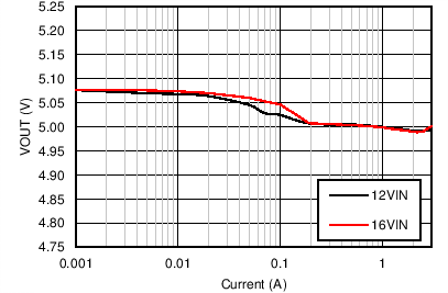
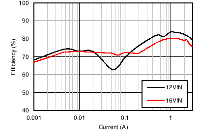
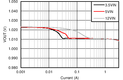
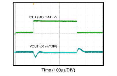
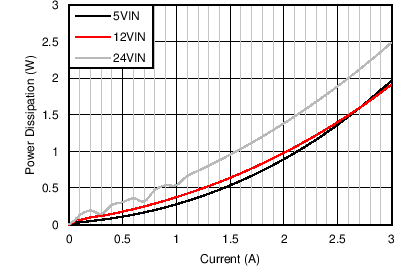
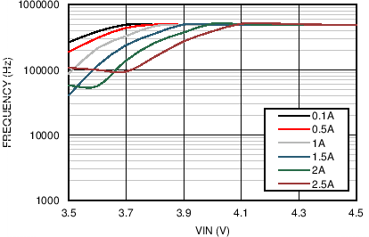
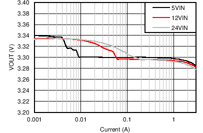
Unless otherwise specified, VIN = 12 V, VOUT = 3.3 V, FS = 500 kHz and room temperature. See below for component values for each VOUT and FS combination.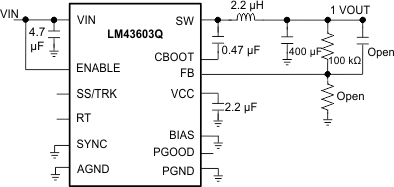
| VOUT = 1 V | FS = 500 kHz |
FS = 500 kHz
| VOUT = 1 V | FS = 500 kHz |
| VIN = 12 V | VOUT = 1 V |
| VOUT = 3.3 V | FS = 500 kHz |
FS = 500 kHz
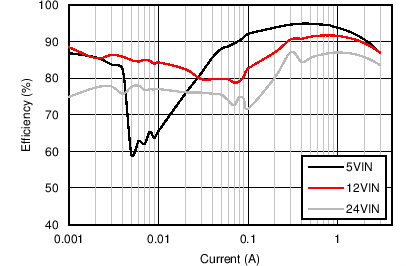
| VOUT = 3.3 V | FS = 500 kHz |
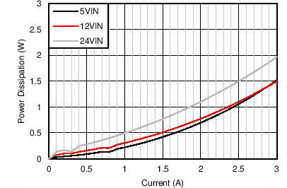
| VOUT = 3.3 V | FS = 500 kHz |
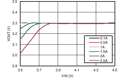
| VOUT = 3.3 V | FS = 500 kHz |
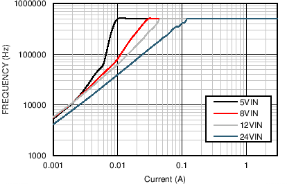
| VOUT = 3.3 V | FS = 500 kHz |
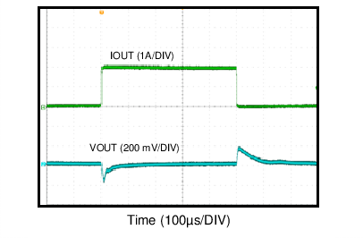
| VOUT = 3.3 V | FS = 500 kHz |
| VOUT = 5 V | FS = 200 kHz |
FS = 200 kHz
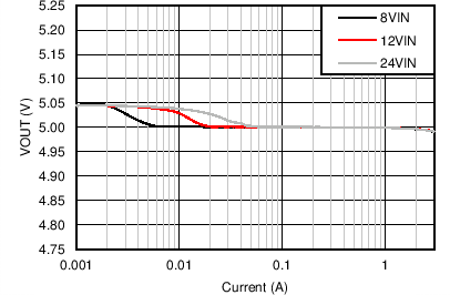
| VOUT = 5 V | FS = 200 kHz |
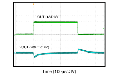
| VOUT = 5 V | FS = 200 kHz |
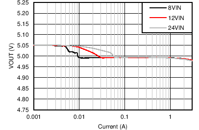
| VOUT = 5 V | FS = 500 kHz |
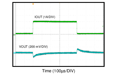
| VOUT = 5 V | FS = 500 kHz |
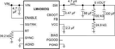
| VOUT = 5 V | FS = 1 MHz |
FS = 1 MHz
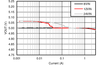
| VOUT = 5 V | FS = 1 MHz |
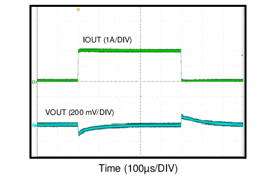
| VOUT = 5 V | FS = 1 MHz |
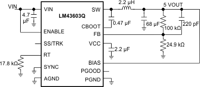
| VOUT = 5 V | FS = 2.2 MHz |
FS = 2.2 MHz
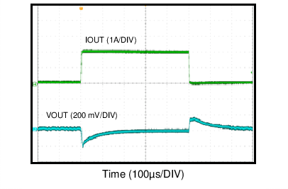
| VOUT = 5 V | FS = 2.2 MHz |
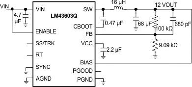
| VOUT = 12 V | FS = 500 kHz |
FS = 500 kHz
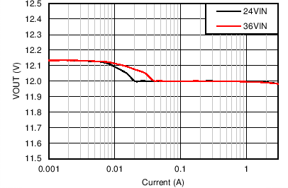
| VOUT = 12 V | FS = 500 kHz |
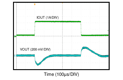
| VOUT = 12 V | FS = 500 kHz | VIN = 24 V |
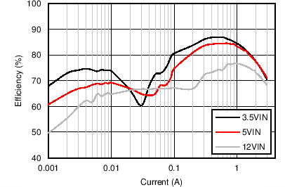
| VOUT = 1 V | Fs = 500 kHz |
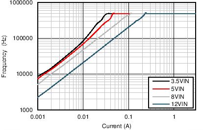
| VOUT = 1 V | FS = 500 kHz |

| VOUT = 1 V | FS = 500 kHz | RθJA = 20°C/W |
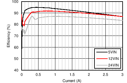
| VOUT = 3.3 V | FS = 500 kHz |
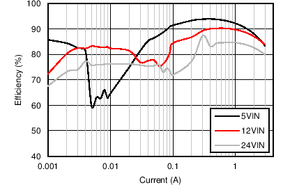
| VOUT = 3.3 V | FS = 500 kHz |
| VOUT = 3.3 V | FS = 500 kHz |
| VOUT = 3.3 V | FS = 500 kHz |
| VOUT = 3.3 V | FS = 500 kHz |
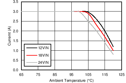
| VOUT = 3.3 V | FS = 500 kHz | RθJA = 20°C/W |
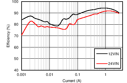
| VOUT = 5 V | FS = 200 kHz |
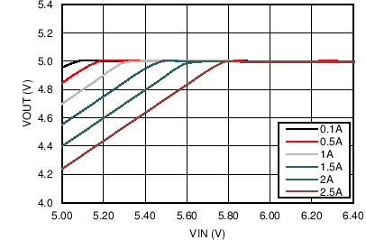
| VOUT = 5 V | FS = 200 kHz |
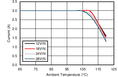
| VOUT = 5 V | FS = 200 kHz | RθJA = 20°C/W |
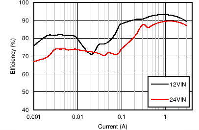
| VOUT = 5 V | FS = 500 kHz |
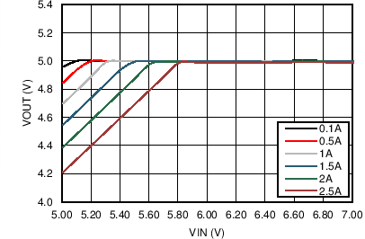
| VOUT = 5 V | FS = 500 kHz |
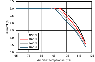
| VOUT = 5 V | FS = 500 kHz | RθJA = 20°C/W |
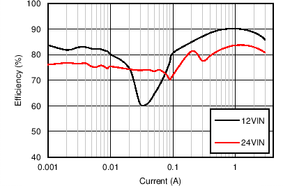
| VOUT = 5 V | FS = 1 MHz |
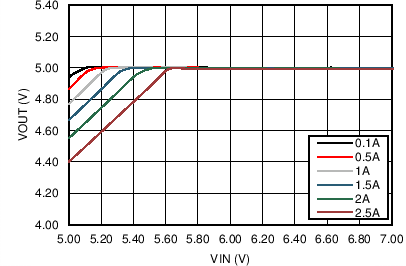
| VOUT = 5 V | FS = 1 MHz |
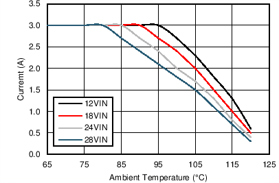
| VOUT = 5 V | FS = 1 MHz | RθJA = 20°C/W |
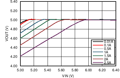
| VOUT = 5 V | FS = 2.2 MHz |
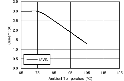
| VOUT = 5 V | FS = 2.2 MHz | RθJA = 20°C/W |
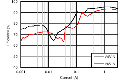
| VOUT = 12 V | FS = 500 kHz |
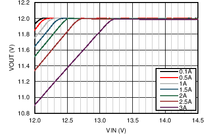
| VOUT = 12 V | FS = 500 kHz |
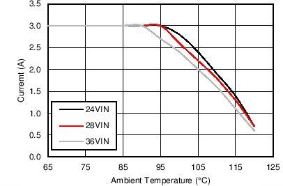
| VOUT = 12 V | FS = 500 kHz | RθJA = 20°C/W |
