SNAS598B July 2012 – July 2015 LM4549B
PRODUCTION DATA.
- 1 Features
- 2 Applications
- 3 Description
- 4 Revision History
- 5 Description (continued)
- 6 Pin Configuration and Functions
- 7 Specifications
-
8 Detailed Description
- 8.1 Overview
- 8.2 Functional Block Diagram
- 8.3 Feature Description
- 8.4 Device Functional Modes
- 8.5
Programming
- 8.5.1
AC Link Serial Interface Protocol
- 8.5.1.1 AC Link Output Frame: SDATA_OUT, Controller Output to LM4549B Input
- 8.5.1.2
AC Link Input Frame: SDATA_IN, Controller Input from LM4549B Output
- 8.5.1.2.1 SDATA_IN: Slot 0 - Codec/Slot Status Bits
- 8.5.1.2.2 SDATA_IN: Slot 1 - Status Address / Slot Request Bits
- 8.5.1.2.3 SDATA_IN: Slot 2 - Status Data
- 8.5.1.2.4 SDATA_IN: Slot 3 - PCM Record Left Channel
- 8.5.1.2.5 SDATA_IN: Slot 4 - PCM Record Right Channel
- 8.5.1.2.6 SDATA_IN: Slots 5 to 12 - Reserved
- 8.5.2 Multiple Codecs
- 8.5.1
AC Link Serial Interface Protocol
- 8.6
Register Maps
- 8.6.1 Reset Register (00h)
- 8.6.2 Master Volume Register (02h)
- 8.6.3 Line Level Volume Register (04h)
- 8.6.4 Mono Volume Register (06h)
- 8.6.5 PC Beep Volume Register (0Ah)
- 8.6.6 Mixer Input Volume Registers (Index 0Ch - 18h)
- 8.6.7 Record Select Register (1Ah)
- 8.6.8 Record Gain Register (1Ch)
- 8.6.9 General Purpose Register (20h)
- 8.6.10 3D Control Register (22h)
- 8.6.11 Power-Down Control / Status Register (26h)
- 8.6.12 Extended Audio ID Register (28h)
- 8.6.13 Extended Audio Status/Control register (2Ah)
- 8.6.14 Sample Rate Control Registers (2Ch, 32h)
- 8.6.15 Vendor ID Registers (7Ch, 7Eh)
- 8.6.16 Reserved Registers
- 9 Application and Implementation
- 10Power Supply Recommendations
- 11Layout
- 12Device and Documentation Support
- 13Mechanical, Packaging, and Orderable Information
Package Options
Mechanical Data (Package|Pins)
- PT|48
Thermal pad, mechanical data (Package|Pins)
Orderable Information
9 Application and Implementation
NOTE
Information in the following applications sections is not part of the TI component specification, and TI does not warrant its accuracy or completeness. TI’s customers are responsible for determining suitability of components for their purposes. Customers should validate and test their design implementation to confirm system functionality.
9.1 Application Information
The LM4549B is an audio codec used for PC systems. It is typically used in systems which are fully PC99-compliant and performs analog functions of the AC '97 Rev 2.1 architecture.
9.2 Typical Application
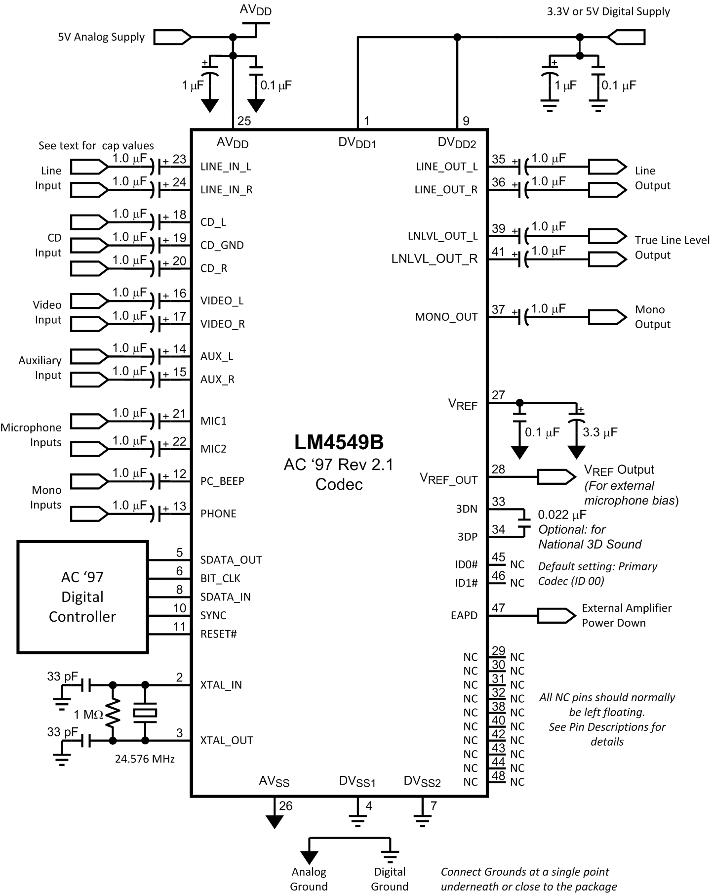
 Figure 21. LM4549B Typical Application Circuit, Single Codec, 1-Vrms Inputs
9.2.1 Design Requirements
For this example the following application parameters exist:
- Single Codec Output
- 1-Vrms input
This design is provided for a high-quality audio path and provides all analog functionality for a PC audio system.
The design has a single codec output with 1-Vrms input.
9.2.2 Detailed Design Procedure
For all analog inputs a 1-uF capacitor should be tied to the input for proper decoupling. If the pin is unused then a 1-uF capacitor should be used and tied to ground.
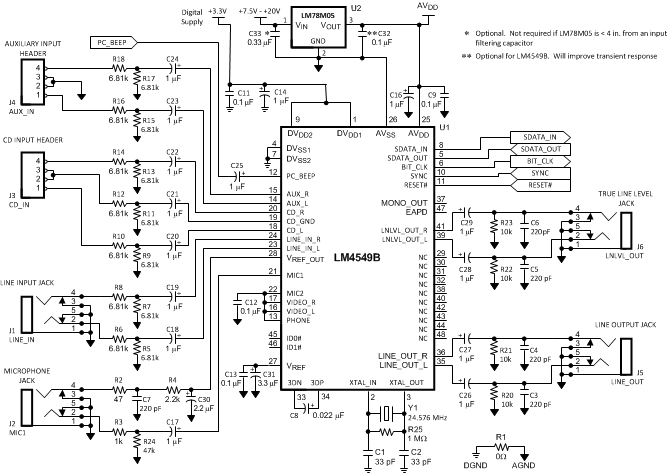
For analog input pins, a proper lowpass filter will be needed to filter out any high frequencies depending on the application. Please see Figure 22.
Digital and Analog voltage supplies should have proper decoupling capacitors that cover low- and high-frequency spikes. In this application, the user chooses to go with 1-uF and 0.1-uF capacitors.
9.3 System Example
In Figure 22, the LM4549B is integrated into a system with a single code, 1-Vrms and 2-Vrms inputs, and EMC output filters.
 Figure 22. LM4549B Reference Design, Typical Application
9.3.1 Improving System Performance
The audio codec is capable of dynamic range performance in excess of 90 db, but the user must pay careful attention to several factors to achieve this. A primary consideration is keeping analog and digital grounds separate, and connecting them together in only one place. Some designers show the connection as a 0-Ω resistor, which allows naming the nets separately. Although it is possible to use a 2-layer board, TI recommends that a minimum of four layers be used, with the two inside layers being analog ground and digital ground. If EMI is a system consideration, then as many as eight layers have been successfully used. The 12- and 25-MHz. clocks can have significant harmonic content depending on the rise and fall times. Bypass capacitors should be very close to the package. The analog VDD pins should be supplied from a separate regulator to reduce noise. By operating the digital portion on 3.3 V instead of 5 V, an additional 0.5- to 0.7-db improvement can be obtained.
The bandgap reference and the anti-pop slow turnon circuit were improved in the LM4549B. A pullup resistor is not required on VREF, pin 27. For an existing design, the 10-kΩ resistor can be left on the PCB, but the temperature coefficient will improve with no resistor on this pin. In addition, the THD will improve by 0.2–0.5 dB. The external capacitor is charged by an internal current source, ramping the voltage slowly. This results in slow turn-on of the audio stages, eliminating “pops and clicks”. Thus, turn-on performance is also improved. The pullup resistor, in conjunction with the internal impedance and the external capacitor, form a frequency dependent divider from the analog supply. Noise on the analog supply will be coupled into the audio path, with approximately 30 dB. of attenuation. Although this is not a large amount if the noise on the supply is tens of millivolts, it will prevent SNR from exceeding 80 dB.
In Figure 21 and Figure 22, the input coupling capacitors are shown as 1-µF capacitors. This is only necessary for extending the response down to 20 Hz. for music applications. For telematics or voice applications, the lower 3-dB point can be much higher. Using a specified input resistance of 10 kΩ, (40 kΩ typical), a 0.1-µF capacitor may be used. The lower 3-dB point will still be below 300 Hz. By using a smaller capacitor, the package size may be reduced, leading to a lower system cost.