SNAS598B July 2012 – July 2015 LM4549B
PRODUCTION DATA.
- 1 Features
- 2 Applications
- 3 Description
- 4 Revision History
- 5 Description (continued)
- 6 Pin Configuration and Functions
- 7 Specifications
-
8 Detailed Description
- 8.1 Overview
- 8.2 Functional Block Diagram
- 8.3 Feature Description
- 8.4 Device Functional Modes
- 8.5
Programming
- 8.5.1
AC Link Serial Interface Protocol
- 8.5.1.1 AC Link Output Frame: SDATA_OUT, Controller Output to LM4549B Input
- 8.5.1.2
AC Link Input Frame: SDATA_IN, Controller Input from LM4549B Output
- 8.5.1.2.1 SDATA_IN: Slot 0 - Codec/Slot Status Bits
- 8.5.1.2.2 SDATA_IN: Slot 1 - Status Address / Slot Request Bits
- 8.5.1.2.3 SDATA_IN: Slot 2 - Status Data
- 8.5.1.2.4 SDATA_IN: Slot 3 - PCM Record Left Channel
- 8.5.1.2.5 SDATA_IN: Slot 4 - PCM Record Right Channel
- 8.5.1.2.6 SDATA_IN: Slots 5 to 12 - Reserved
- 8.5.2 Multiple Codecs
- 8.5.1
AC Link Serial Interface Protocol
- 8.6
Register Maps
- 8.6.1 Reset Register (00h)
- 8.6.2 Master Volume Register (02h)
- 8.6.3 Line Level Volume Register (04h)
- 8.6.4 Mono Volume Register (06h)
- 8.6.5 PC Beep Volume Register (0Ah)
- 8.6.6 Mixer Input Volume Registers (Index 0Ch - 18h)
- 8.6.7 Record Select Register (1Ah)
- 8.6.8 Record Gain Register (1Ch)
- 8.6.9 General Purpose Register (20h)
- 8.6.10 3D Control Register (22h)
- 8.6.11 Power-Down Control / Status Register (26h)
- 8.6.12 Extended Audio ID Register (28h)
- 8.6.13 Extended Audio Status/Control register (2Ah)
- 8.6.14 Sample Rate Control Registers (2Ch, 32h)
- 8.6.15 Vendor ID Registers (7Ch, 7Eh)
- 8.6.16 Reserved Registers
- 9 Application and Implementation
- 10Power Supply Recommendations
- 11Layout
- 12Device and Documentation Support
- 13Mechanical, Packaging, and Orderable Information
Package Options
Mechanical Data (Package|Pins)
- PT|48
Thermal pad, mechanical data (Package|Pins)
Orderable Information
7 Specifications
7.1 Absolute Maximum Ratings
over operating free-air temperature range (unless otherwise noted)(1)(9)| MIN | MAX | UNIT | |||
|---|---|---|---|---|---|
| Supply Voltage | 6 | 6 | V | ||
| Input Voltage | −0.3 | VDD +0.3 | V | ||
| Junction Temperature | 150 | °C | |||
| Soldering Information | Vapor Phase (60 sec.) | 215 | °C | ||
| Infrared (15 sec.) | 220 | ||||
| Storage Temperature, Tstg | –65 | 150 | °C | ||
(1) Stresses beyond those listed under Absolute Maximum Ratings may cause permanent damage to the device. These are stress ratings only, which do not imply functional operation of the device at these or any other conditions beyond those indicated under Recommended Operating Conditions. Exposure to absolute-maximum-rated conditions for extended periods may affect device reliability.
7.2 ESD Ratings
| VALUE | UNIT | ||||
|---|---|---|---|---|---|
| V(ESD) | Electrostatic discharge | Human-body model (HBM), per ANSI/ESDA/JEDEC JS-001(1) | All pins except 3 | ±2000 | V |
| Pin 3 | ±750 | ||||
| Machine Model (MM) | All pins except 3 | ±200 | |||
| Pin 3 | ±100 | ||||
(1) JEDEC document JEP155 states that 500-V HBM allows safe manufacturing with a standard ESD control process.
7.3 Recommended Operating Conditions
over operating free-air temperature range (unless otherwise noted)| MIN | MAX | UNIT | ||
|---|---|---|---|---|
| Temperature TMIN ≤ TA ≤ TMAX(2) | −40 | 85 | °C | |
| Analog Supply | 4.2 | 5.5 | V | |
| Digital Supply | 3 | 5.5 | V | |
7.4 Thermal Information
| THERMAL METRIC(1) | LM4549B | UNIT | |
|---|---|---|---|
| PT (LQFP) | |||
| 48 PINS | |||
| RθJA | Junction-to-ambient thermal resistance | 74 | °C/W |
(1) For more information about traditional and new thermal metrics, see the Semiconductor and IC Package Thermal Metrics application report, SPRA953.
7.5 Electrical Characteristics
The following specifications apply for AVDD = 5 V, DVDD = 3.3 V, Fs = 48 kHz, single codec configuration, (primary mode) unless otherwise noted. Limits apply for TA= 25°C. The reference for 0 dB is 1 Vrms unless otherwise specified.(1)(3)| PARAMETER | TEST CONDITIONS | MIN | TYP(4) | MAX(5) | UNIT | |
|---|---|---|---|---|---|---|
| AVDD | Analog Supply | 4.2 | 5.5 | V | ||
| DVDD | Digital Supply | 3 | 5.5 | V | ||
| DIDD | Digital Quiescent Power Supply Current | DVDD = 5 V | 34 | mA | ||
| DVDD = 3.3 V | 19 | |||||
| AIDD | Analog Quiescent Power Supply Current | AVDD = 5.5 V | 53 | mA | ||
| IDSD | Digital Shutdown Current | PR543210 = 111111 | 19 | µA | ||
| IASD | Analog Shutdown Current | PR543210 = 111111 | 70 | µA | ||
| VREF | Reference Voltage | No pullup resistor | 2.16 | V | ||
| PSRR | Power Supply Rejection Ratio | 40 | dB | |||
| ANALOG LOOPTHROUGH MODE(6) | ||||||
| Dynamic(7) | CD Input to Line Output, -60 dB Input THD+N | 90 | 97 | dB | ||
| THD | Total Harmonic Distortion | VO = -3 dB, f = 1 kHz, RL = 10 kΩ | 0.013% | 0.02% | ||
| ANALOG INPUT SECTION | ||||||
| VIN | Line Input Voltage | LINE_IN, AUX, CD, VIDEO, PC_BEEP, PHONE | 1 | Vrms | ||
| VIN | Mic Input with 20 dB Gain | 0.1 | Vrms | |||
| VIN | Mic Input with 0 dB Gain | 1 | Vrms | |||
| Xtalk | Crosstalk | CD Left to Right | -95 | dB | ||
| ZIN | Input Impedance(7) | All Analog Inputs | 10 | 40 | kΩ | |
| CIN | Input Capacitance(7) | 3.7 | 7 | pF | ||
| Interchannel Gain Mismatch | CD Left to Right | 0.1 | dB | |||
| RECORD GAIN AMPLIFIER - ADC | ||||||
| AS | Step Size | 0 dB to 22.5 dB | 1.5 | dB | ||
| AM | Mute Attenuation(7) | 86 | dB | |||
| MIXER SECTION | ||||||
| AS | Step Size | +12 dB to -34.5 dB | 1.5 | dB | ||
| AM | Mute Attenuation | 86 | dB | |||
| ANALOG TO DIGITAL CONVERTERS | ||||||
| Resolution | 18 | Bits | ||||
| Dynamic(7) | -60 dB Input THD+N, A-Weighted | 86 | 90 | dB | ||
| Frequency Response | -1 dB Bandwidth | 20 | kHz | |||
| DIGITAL TO ANALOG CONVERTERS | ||||||
| Resolution | 18 | Bits | ||||
| Dynamic(7) | -60 dB Input THD+N, A-Weighted | 82 | 89 | dB | ||
| THD | Total Harmonic Distortion | VIN = -3 dB, f = 1 kHz, RL = 10 kΩ | 0.01% | |||
| Frequency Response | 20 - 21 | kHz | ||||
| Group Delay(7) | Sample Frequency = 48 kHz | 0.36 | 1 | ms | ||
| Out of Band Energy(8) | -40 | dB | ||||
| Stop Band Rejection | 70 | dB | ||||
| DT | Discrete Tones | -96 | dB | |||
| ANALOG OUTPUT SECTION | ||||||
| AS | Step Size | 0 dB to -46.5 dB | 1.5 | dB | ||
| AM | Mute Attenuation | 86 | dB | |||
| ZOUT | Output Impedance(7) | All Analog Outputs | 220 | Ω | ||
| DIGITAL I/O(7) | ||||||
| VIH | High level input voltage | 0.65 x DVDD | V | |||
| VIL | Low level input voltage | 0.35 x DVDD | V | |||
| VOH | High level output voltage | IO = 2.5 mA | 0.90 x DVDD | V | ||
| VOL | Low level output voltage | IO = 2.5 mA | 0.10 x DVDD | V | ||
| IL | Input Leakage Current | AC Link inputs | ±10 | µA | ||
| IL | Tri state Leakage Current | High impedance AC Link outputs | ±10 | µA | ||
| CIN | AC-Link I/O capacitance(7) | SDout, BitClk, SDin, Sync, Reset# only | 4 | 7.5 | pF | |
| IDR | Output drive current | AC Link outputs | 5 | mA | ||
(1) Absolute Maximum Ratings indicate limits beyond which damage to the device may occur. Operating Ratings indicate conditions for which the device is functional, but do not ensure specific performance limits. Electrical Characteristics state DC and AC electrical specifications under particular test conditions which ensure specific performance limits. This assumes that the device is within the Operating Ratings. Specifications are not ensured for parameters where no limit is given, however, the typical value is a good indication of device performance.
(2) The maximum power dissipation must be derated at elevated temperatures and is dictated by TJMAX, RθJA, and the ambient temperature TA. The maximum allowable power dissipation is PDMAX = (TJMAX– TA)/RθJA or the number given in Absolute Maximum Ratings, whichever is lower. For the LM4549B, TJMAX = 150°C. The typical junction-to-ambient thermal resistance is 74°C/W for package number PT0048A.
(3) All voltages are measured with respect to the ground pin, unless otherwise specified.
(4) Typicals are measured at 25°C and represent the parametric norm.
(5) Limits are specified to AOQL (Average Outgoing Quality Level).
(6) Loopthrough mode describes a path from an analog input through the analog mixer to an analog output
(7) These specifications are ensured by design and characterization; they are not production tested.
(8) Out of band energy is measured from 28.8 kHz to 100 kHz relative to a 1-Vrms DAC output.
(9) If Military/Aerospace specified devices are required, please contact the Texas Instruments Sales Office/ Distributors for availability and specifications.
7.6 Timing Requirements
| MIN | NOM | MAX | UNIT | |||
|---|---|---|---|---|---|---|
| FBC | BIT_CLK frequency | 12.288 | MHz | |||
| TBCP | BIT_CLK period | 81.4 | ns | |||
| TCH | BIT_CLK high | Variation of BIT_CLK duty cycle from 50% | ±20% | |||
| FSYNC | SYNC frequency | 48 | kHz | |||
| TSP | SYNC period | 20.8 | µs | |||
| TSH | SYNC high pulse width | 1.3 | µs | |||
| TSL | SYNC low pulse width | 19.5 | µs | |||
| TDSETUP | Setup Time for codec data input | SDATA_OUT to falling edge of BIT_CLK | 10 | 3.5 | ns | |
| TDHOLD | Hold Time for codec data input(1) | Hold time of SDATA_OUT from falling edge of BIT_CLK | 10 | 5.3 | ns | |
| TSSETUP | Setup Time for codec SYNC input(1) | SYNC to falling edge of BIT_CLK | 10 | 3.8 | ns | |
| TSHOLD | Hold Time for codec SYNC input(1) | Hold time of SYNC from falling edge of BIT_CLK | 10 | ns | ||
| TCO | Output Valid Delay | Output Delay of SDATA_IN from rising edge of BIT_CLK | 5.2 | 15 | ns | |
| TRISE | Rise Time(1) | BIT_CLK, SYNC, SDATA_IN or SDATA_OUT | 6 | ns | ||
| TFALL | Fall Time(1) | BIT_CLK, SYNC, SDATA_IN or SDATA_OUT | 6 | ns | ||
| TRST_LOW | RESET# active low pulse width(1) | For Cold Reset | 1 | µs | ||
| TRST2CLK | RESET# inactive to BIT_CLK start up | For Cold Reset | 162.8 | 271 | ns | |
| TSH | SYNC active high pulse width(1) | For Warm Reset | 1 | µs | ||
| TSYNC2CLK | SYNC inactive to BIT_CLK start up | For Warm Reset | 162.8 | ns | ||
| TS2_PDOWN | AC Link Power Down Delay | Delay from end of Slot 2 to BIT_CLK, SDATA_IN low | 1 | µs | ||
| TSUPPLY2RST | Power-On Reset | Time from minimum valid supply levels to end of Reset | 1 | µs | ||
| TSU2RST | Setup to trailing edge of RESET#(1) | For ATE Test Mode | 15 | ns | ||
| TRST2HZ | Rising edge of RESET# to Hi-Z(1) | For ATE Test Mode | 25 | ns | ||
(1) These specifications are ensured by design and characterization; they are not production tested.
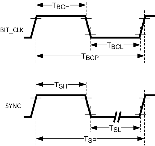 Figure 1. Clocks
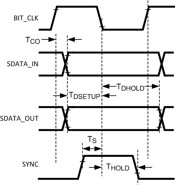 Figure 2. Data Delay, Setup and Hold
 Figure 3. Digital Rise and Fall
 Figure 4. Legend
 Figure 5. Power-On Reset
 Figure 6. Cold Reset
 Figure 7. Warm Reset
7.7 Typical Characteristics
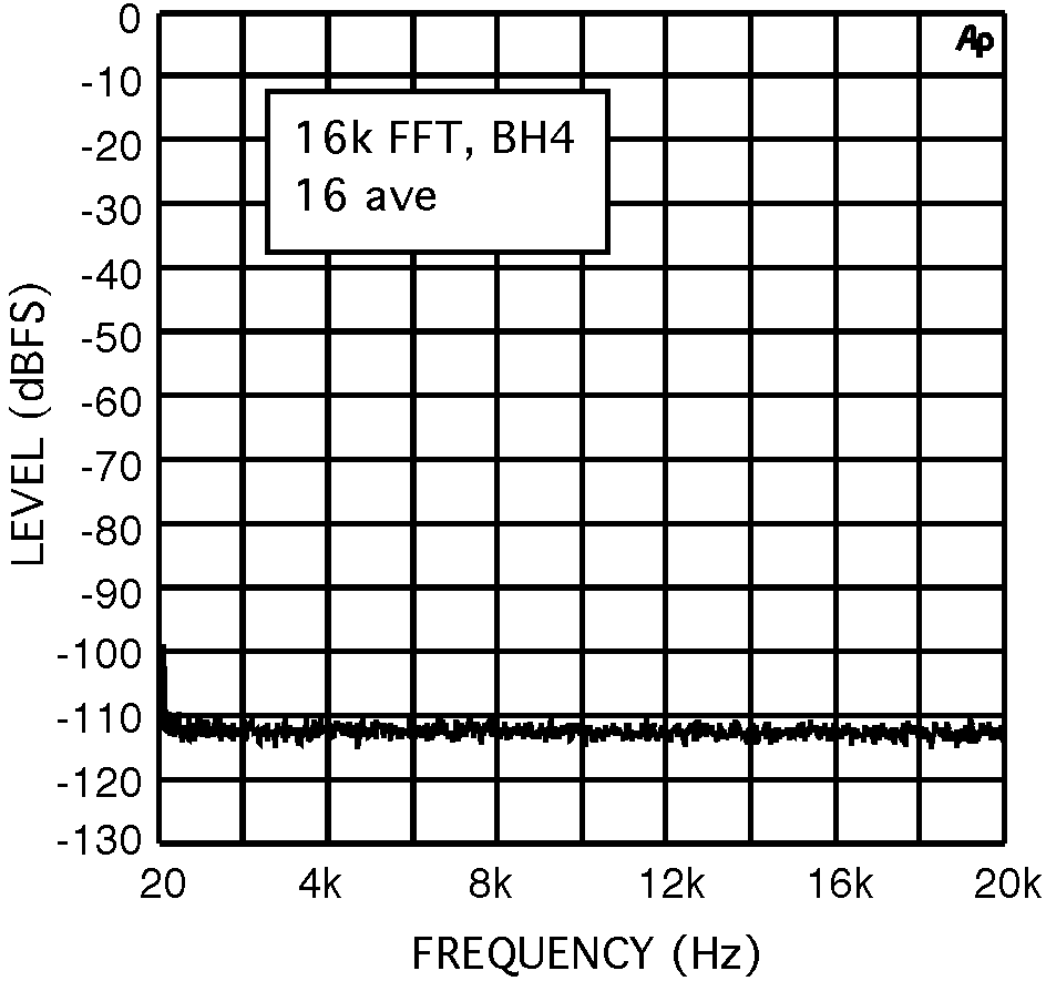 Figure 8. ADC Noise Floor
 Figure 10. Line Out Noise Floor (Analog Loopthrough)
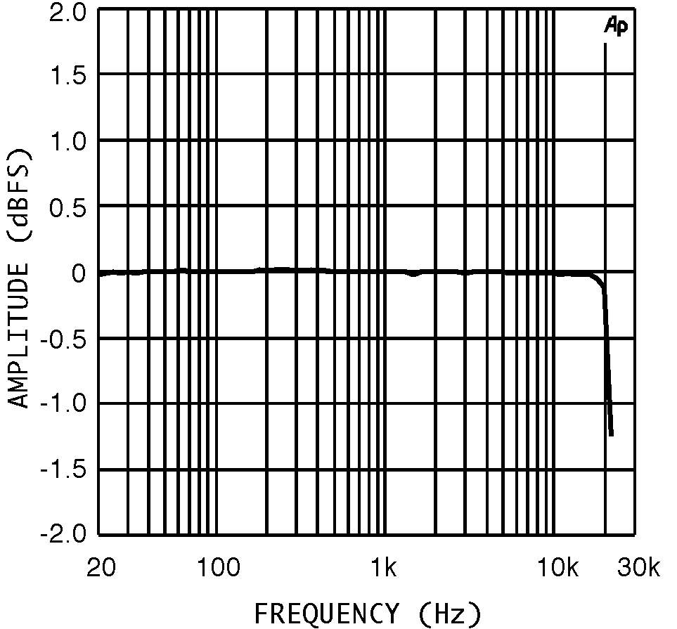 Figure 12. ADC Frequency Response
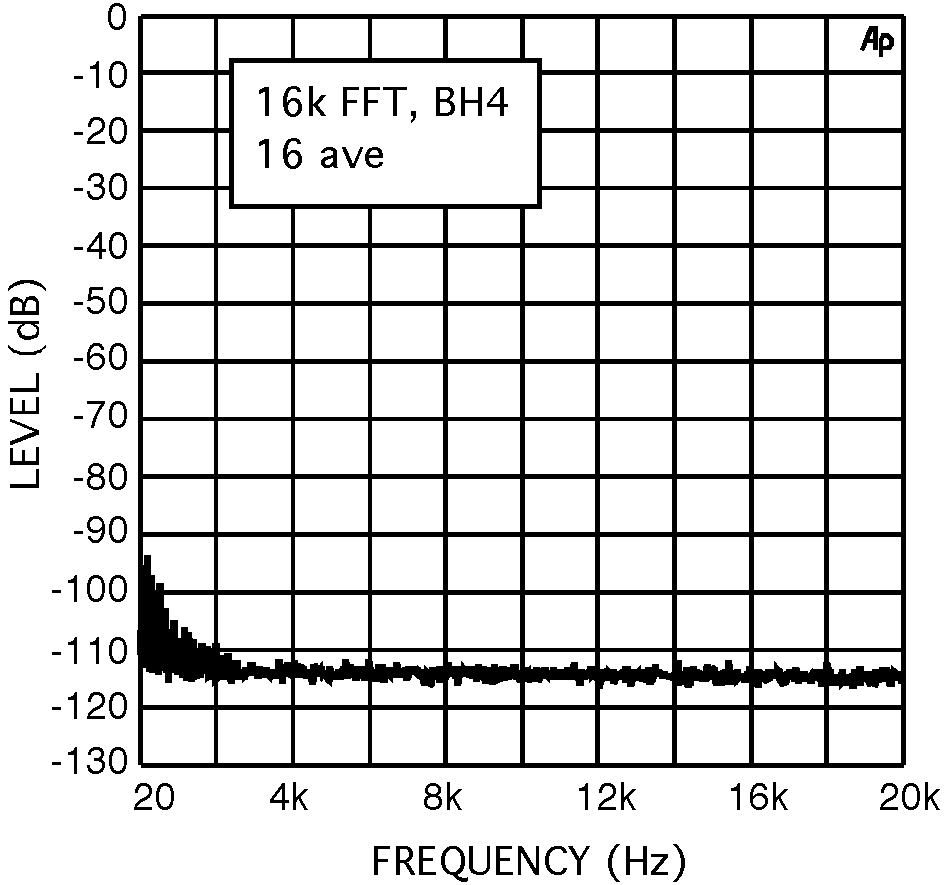 Figure 9. DAC Noise Floor
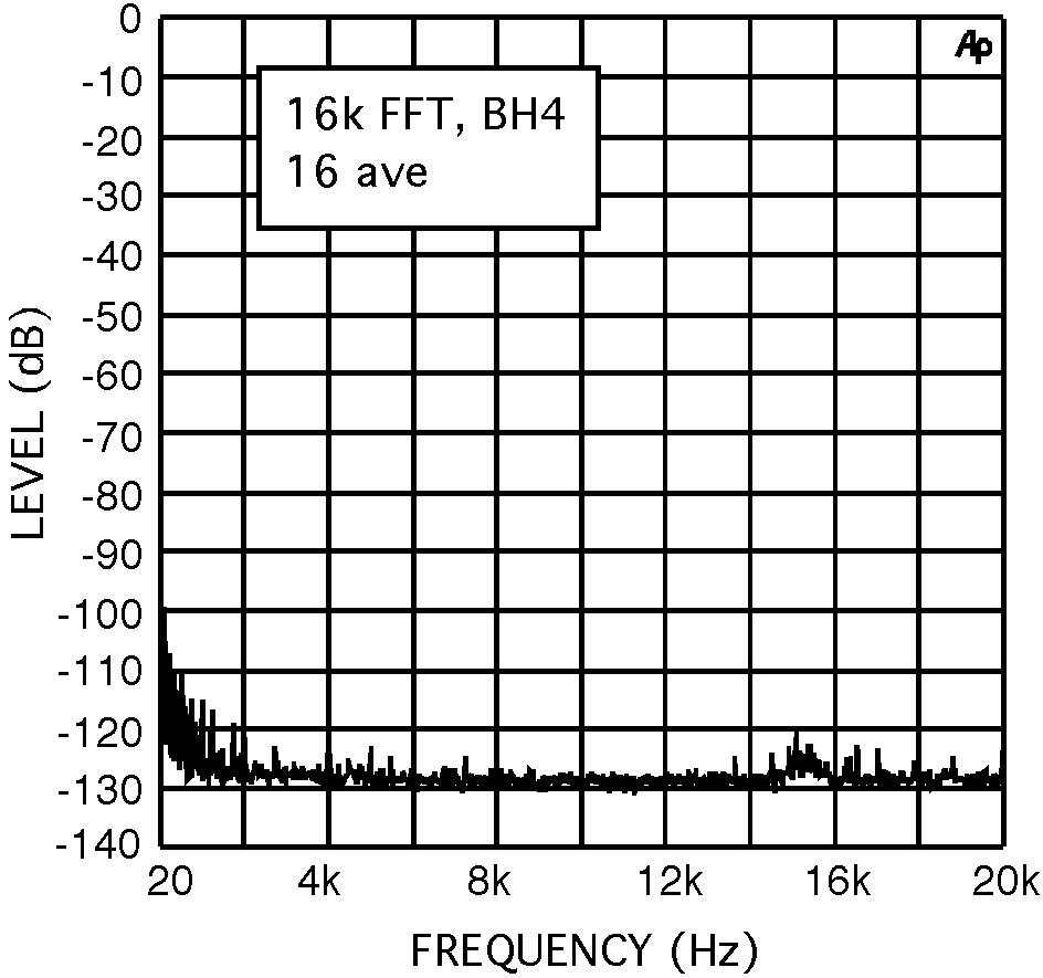 Figure 11. Line Level Out Noise Floor (Analog Loopthrough)
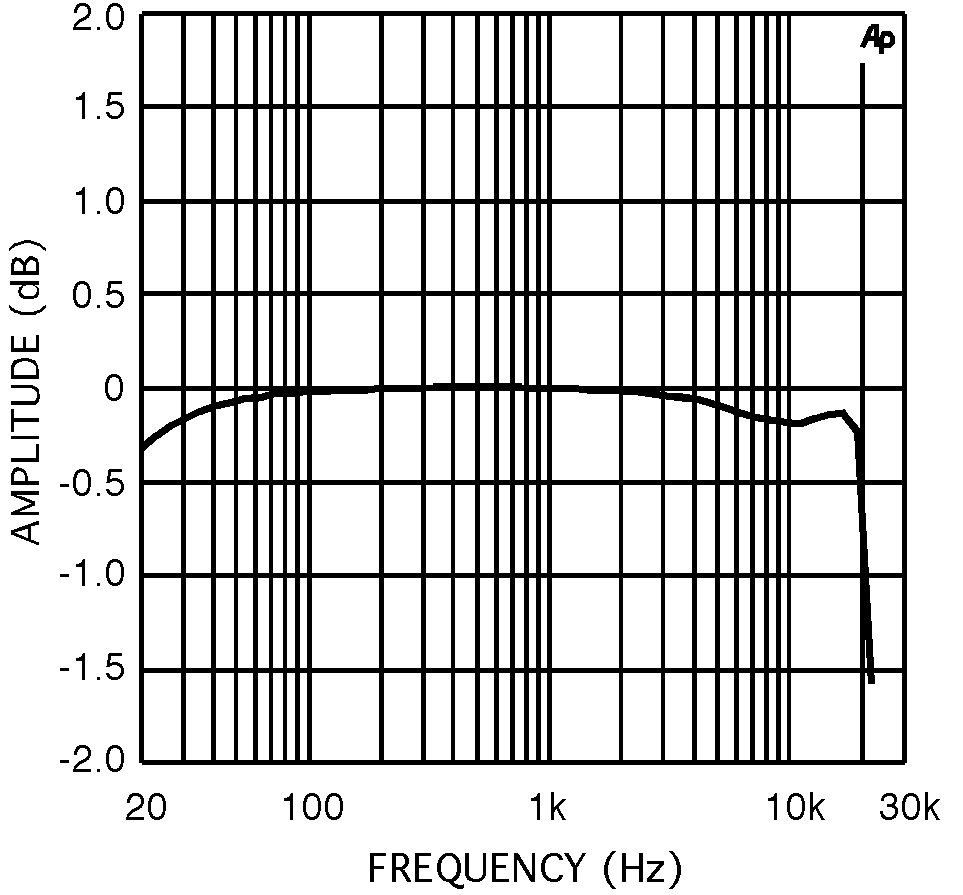 Figure 13. DAC Frequency Response