SNVSAA3B July 2015 – November 2017 LM46001-Q1
PRODUCTION DATA.
- 1 Features
- 2 Applications
- 3 Description
- 4 Revision History
- 5 Pin Configuration and Functions
- 6 Specifications
-
7 Detailed Description
- 7.1 Overview
- 7.2 Functional Block Diagram
- 7.3
Feature Description
- 7.3.1 Fixed Frequency Peak Current Mode Controlled Step-Down Regulator
- 7.3.2 Light Load Operation
- 7.3.3 Adjustable Output Voltage
- 7.3.4 Enable (ENABLE)
- 7.3.5 VCC, UVLO and BIAS
- 7.3.6 Soft Start and Voltage Tracking (SS/TRK)
- 7.3.7 Switching Frequency (RT) and Synchronization (SYNC)
- 7.3.8 Minimum ON-Time, Minimum OFF-Time and Frequency Foldback at Dropout Conditions
- 7.3.9 Internal Compensation and CFF
- 7.3.10 Bootstrap Voltage (BOOT)
- 7.3.11 Power Good (PGOOD)
- 7.3.12 Overcurrent and Short Circuit Protection
- 7.3.13 Thermal Shutdown
- 7.4 Device Functional Modes
-
8 Applications and Implementation
- 8.1 Application Information
- 8.2
Typical Applications
- 8.2.1 Design Requirements
- 8.2.2
Detailed Design Procedure
- 8.2.2.1 Custom Design With WEBENCH® Tools
- 8.2.2.2 Output Voltage Setpoint
- 8.2.2.3 Switching Frequency
- 8.2.2.4 Input Capacitors
- 8.2.2.5 Inductor Selection
- 8.2.2.6 Output Capacitor Selection
- 8.2.2.7 Feed-Forward Capacitor
- 8.2.2.8 Bootstrap Capacitors
- 8.2.2.9 VCC Capacitor
- 8.2.2.10 BIAS Capacitors
- 8.2.2.11 Soft-Start Capacitors
- 8.2.2.12 Undervoltage Lockout Set-Point
- 8.2.2.13 PGOOD
- 8.2.3 Application Performance Curves
- 9 Power Supply Recommendations
- 10Layout
- 11Device and Documentation Support
- 12Mechanical, Packaging, and Orderable Information
Package Options
Mechanical Data (Package|Pins)
- PWP|16
Thermal pad, mechanical data (Package|Pins)
- PWP|16
Orderable Information
6 Specifications
6.1 Absolute Maximum Ratings
Over operating free-air temperature range (unless otherwise noted)(1)| PARAMETER | MIN | MAX | UNIT | |
|---|---|---|---|---|
| Input voltages | VIN to PGND | –0.3 | 65 | V |
| EN to PGND | –0.3 | VIN + 0.3 | ||
| FB, RT, SS/TRK to AGND | –0.3 | 3.6 | ||
| PGOOD to AGND | –0.3 | 15 | ||
| SYNC to AGND | –0.3 | 5.5 | ||
| BIAS to AGND | –0.3 | 30 | ||
| AGND to PGND | –0.3 | 0.3 | ||
| Output voltages | SW to PGND | –0.3 | VIN + 0.3 | V |
| SW to PGND less than 10-ns transients | –3.5 | 65 | ||
| CBOOT to SW | –0.3 | 5.5 | ||
| VCC to AGND | –0.3 | 3.6 | ||
| Storage temperature range, Tstg | –65 | 150 | °C | |
(1) Stresses beyond those listed under Absolute Maximum Ratings may cause permanent damage to the device. These are stress ratings only, and functional operation of the device at these or any other conditions beyond those indicated under Recommended Operating Conditions is not implied. Exposure to absolute-maximum-rated conditions for extended periods may affect device reliability.
6.2 ESD Ratings
| VALUE | UNIT | |||
|---|---|---|---|---|
| V(ESD) | Electrostatic discharge | Human-body model (HBM), per AEC Q100-002(1) | ±2000 | V |
| Charged-device model (CDM), per AEC Q100-011 | ±750 | |||
(1) AEC Q100-002 indicates that HBM stressing shall be in accordance with the ANSI/ESDA/JEDEC JS-001 specification.
6.3 Recommended Operating Conditions
Over operating free-air temperature range (unless otherwise noted)(1)| PARAMETER | MIN | MAX | UNIT | |
|---|---|---|---|---|
| Input voltages | VIN to PGND | 3.5 | 60 | V |
| EN | –0.3 | VIN | ||
| FB | –0.3 | 1.1 | ||
| PGOOD | –0.3 | 12 | ||
| BIAS input not used | –0.3 | 0.3 | ||
| BIAS input used | 3.3 | 28 | ||
| AGND to PGND | –0.1 | 0.1 | ||
| Output voltage adjustable range | VOUT | 1 | 28 | V |
| Output current | IOUT | 0 | 1 | A |
| Temperature | Operating junction temperature range, TJ | –40 | 125 | °C |
(1) Operating Ratings indicate conditions for which the device is intended to be functional, but do not ensure specific performance limits. For ensured specifications, see Electrical Characteristics.
6.4 Thermal Information
| THERMAL METRIC(1)(2) | LM46001-Q1 | UNIT | |
|---|---|---|---|
| PWP (HTSSOP) | |||
| 16 PINS | |||
| RθJA | Junction-to-ambient thermal resistance | 39.9(3) | °C/W |
| RθJC(top) | Junction-to-case (top) thermal resistance | 26.9 | °C/W |
| RθJB | Junction-to-board thermal resistance | 21.7 | °C/W |
| ψJT | Junction-to-top characterization parameter | 0.8 | °C/W |
| ψJB | Junction-to-board characterization parameter | 21.5 | °C/W |
| RθJC(bot) | Junction-to-case (bottom) thermal resistance | 2.3 | °C/W |
(1) For more information about traditional and new thermal metrics, see the Semiconductor and IC Package Thermal Metrics application report.
(2) The package thermal impedance is calculated in accordance with JESD 51-7 standard with a 4-layer board and 1 W power dissipation.
(3) RθJA is highly related to PCB layout and heat sinking. Please refer to Figure 101 for measured RθJA vs PCB area from a 2-layer board and a 4-layer board.
6.5 Electrical Characteristics
Limits apply over the recommended operating junction temperature (TJ) range of –40°C to +125°C, unless otherwise stated. Minimum and maximum limits are specified through test, design or statistical correlation. Typical values represent the most likely parametric norm at TJ = 25°C, and are provided for reference purposes only. Unless otherwise stated, the following conditions apply: VIN = 24 V, VOUT = 3.3 V, FS = 500 kHz.| PARAMETER | TEST CONDITIONS | MIN | TYP | MAX | UNIT | |
|---|---|---|---|---|---|---|
| SUPPLY VOLTAGE (VIN PINS) | ||||||
| VIN-MIN-ST | Minimum input voltage for startup | 3.8 | V | |||
| ISHDN | Shutdown quiescent current | VEN = 0 V | 2.3 | 5 | µA | |
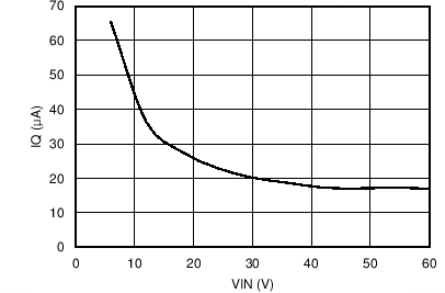
| IQ-NONSW | Operating quiescent current (non-switching) from VIN | VEN = 3.3 V VFB = 1.5 V VBIAS = 3.4 V external |
7 | 13 | µA | |
| IBIAS-NONSW | Operating quiescent current (non-switching) from external VBIAS | VEN = 3.3 V VFB = 1.5 V VBIAS = 3.4 V external |
85 | 140 | µA | |
| IQ-SW | Operating quiescent current (switching) | VEN = 3.3 V IOUT = 0 A RT = open VBIAS = VOUT = 3.3 V RFBT = 1 Meg |
24 | µA | ||
| ENABLE (EN PIN) | ||||||
| VEN-VCC-H | Voltage level to enable the internal LDO output VCC | VENABLE high level | 1.2 | V | ||
| VEN-VCC-L | Voltage level to disable the internal LDO output VCC | VENABLE low level | 0.4 | V | ||
| VEN-VOUT-H | Precision enable level for switching and regulator output: VOUT | VENABLE high level | 2 | 2.1 | 2.42 | V |
| VEN-VOUT-HYS | Hysteresis voltage between VOUT precision enable and disable thresholds | VENABLE hysteresis | –305 | mV | ||
| ILKG-EN | Enable input leakage current | VEN = 3.3 V | 0.8 | 1.75 | µA | |
| INTERNAL LDO (VCC PIN AND BIAS PIN) | ||||||
| VCC | Internal LDO output voltage VCC | VIN ≥ 3.8 V | 3.3 | V | ||
| VCC-UVLO | Undervoltage lockout (UVLO) thresholds for VCC | VCC rising threshold | 3.14 | V | ||
| Hysteresis voltage between rising and falling thresholds | –567 | mV | ||||
| VBIAS-ON | Internal LDO input change over threshold to BIAS | VBIAS rising threshold | 2.96 | 3.2 | V | |
| Hysteresis voltage between rising and falling thresholds | –71 | mV | ||||
| VOLTAGE REFERENCE (FB PIN) | ||||||
| VFB | Feedback voltage | TJ = 25ºC | 1.009 | 1.016 | 1.023 | V |
| TJ = –40ºC to 125ºC | 0.999 | 1.016 | 1.039 | |||
| ILKG-FB | Input leakage current at FB pin | FB = 1.016 V | 0.2 | 65 | nA | |
| THERMAL SHUTDOWN | ||||||
| TSD (1) | Thermal shutdown | Shutdown threshold | 160 | ºC | ||
| Recovery threshold | 150 | |||||
| CURRENT LIMIT AND HICCUP | ||||||
| IHS-LIMIT | Peak inductor current limit | 2.07 | 2.45 | 2.71 | A | |
| ILS-LIMIT | Valley inductor current limit | 0.94 | 1.1 | 1.25 | A | |
| SOFT START (SS/TRK PIN) | ||||||
| ISSC | Soft-start charge current | 1.17 | 2.2 | 2.85 | µA | |
| RSSD | Soft-start discharge resistance | UVLO, TSD, OCP, or EN = 0 V | 16 | kΩ | ||
| POWER GOOD (PGOOD PIN) | ||||||
| VPGOOD-HIGH | Power-good flag overvoltage tripping threshold | % of FB voltage | 110% | 113% | ||
| VPGOOD-LOW | Power-good flag undervoltage tripping threshold | % of FB voltage | 83% | 90% | ||
| VPGOOD-HYS | Power-good flag recovery hysteresis | % of FB voltage | 6% | |||
| RPGOOD | PGOOD pin pulldown resistance when power bad | LM46001-Q1: VEN = 3.3 V | 40 | 125 | Ω | |
| LM46001-Q1: VEN = 0 V | 60 | 150 | ||||
| LM46001A-Q1: VEN = 3.3 V | 69 | 150 | ||||
| LM46001A-Q1: VEN = 0 V | 150 | 350 | ||||
| MOSFETS(2) | ||||||
| RDS-ON-HS | High-side MOSFET ON-resistance | IOUT = 0.5 A VBIAS = VOUT = 3.3 V |
419 | mΩ | ||
| RDS-ON-LS | Low-side MOSFET ON-resistance | IOUT = 0.5 A VBIAS = VOUT = 3.3 V |
231 | mΩ | ||
(1) Ensured by design.
(2) Measured at package pins.
6.6 Timing Requirements
Typical values represent the most likely parametric norm at TJ = 25°C.| MIN | NOM | MAX | UNIT | ||
|---|---|---|---|---|---|
| CURRENT LIMIT AND HICCUP | |||||
| NOC | Hiccup wait cycles when LS current limit tripped | 32 | Cycles | ||
| TOC | Hiccup retry delay time | 5.5 | ms | ||
| SOFT START (SS/TRK PIN) | |||||
| TSS | Internal soft-start time when SS pin open circuit | 4.1 | ms | ||
| POWER GOOD (PGOOD PIN) | |||||
| TPGOOD-RISE | Power-good flag rising transition deglitch delay | 220 | µs | ||
| TPGOOD-FALL | Power-good flag falling transition deglitch delay | 220 | µs | ||
6.7 Switching Characteristics
Limits apply over the recommended operating junction temperature (TJ) range of –40°C to +125°C, unless otherwise stated. Minimum and maximum limits are specified through test, design or statistical correlation. Typical values represent the most likely parametric norm at TJ = 25°C, and are provided for reference purposes only. Unless otherwise stated, the following conditions apply: VIN = 24 V, VOUT = 3.3 V, FS = 500 kHz.| PARAMETER | TEST CONDITIONS | MIN | TYP | MAX | UNIT | |
|---|---|---|---|---|---|---|
| SW (SW PIN) | ||||||
| tON-MIN(1) | Minimum high side MOSFET ON-time | 125 | 165 | ns | ||
| tOFF-MIN(1) | Minimum high side MOSFET OFF-time | 200 | 250 | ns | ||
| OSCILLATOR (SW PINS AND SYNC PIN) | ||||||
| FOSC-DEFAULT | Oscillator default frequency | RT pin open circuit | 445 | 500 | 570 | kHz |
| FADJ | Minimum adjustable frequency | With 1% resistors at RT pin | 200 | kHz | ||
| Maximum adjustable frequency | 2200 | kHz | ||||
| Frequency adjust accuracy | 10% | |||||
| VSYNC-HIGH | Sync clock high level threshold | 2 | V | |||
| VSYNC-LOW | Sync clock low level threshold | 0.4 | V | |||
| DSYNC-MAX | Sync clock maximum duty cycle | 90% | ||||
| DSYNC-MIN | Sync clock minimum duty cycle | 10% | ||||
| TSYNC-MIN | Minimum sync clock ON- and OFF-time | 80 | ns | |||
(1) Ensured by design.
6.8 Typical Characteristics
Unless otherwise specified, VIN = 24 V, VOUT = 3.3 V, FS = 500 kHz, L = 18 µH, COUT = 100 µF, CFF = 33 pF. See Application Performance Curves for bill of materials (BOM) for other VOUT and FS combinations.
| VOUT = 3.3 V | FS = 500 kHz |

| VOUT = 5 V | FS = 200 kHz |

| VOUT = 12 V | FS = 500 kHz |

| VOUT = 3.3 V | FS = 500 kHz |

| VOUT = 5 V | FS = 200 kHz |

| VOUT = 12 V | FS = 500 kHz |

| VOUT = 3.3 V | FS = 500 kHz |

| VOUT = 5 V | FS = 200 kHz |

| VOUT = 12 V | FS = 500 kHz |
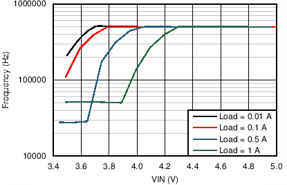
| VOUT = 3.3 V | FS = 500 kHz |

| VOUT = 3.3 V | FS = 500 kHz | IOUT = 1 A |
| Measured on the LM46001QPWPEVM with default BOM. No input filter used. | ||

| VOUT = 3.3 V | FS = 500 kHz | IOUT = 1 A |
| Measured on the LM46001QPWPEVM with default BOM. EVM input filter: Lin = 1 µH Cd = 47 µF CIN4 = 68 µF | ||

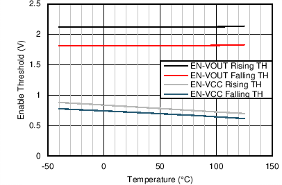


| VIN = 24 V | VOUT = 3.3 V | FS = 500 kHz |

| VOUT = 5 V | FS = 500 kHz |

| VOUT = 5 V | FS = 1 MHz |

| VOUT = 24 V | FS = 500 kHz |

| VOUT = 5 V | FS = 500 kHz |

| VOUT = 5 V | FS = 1 MHz |

| VOUT = 24 V | FS = 500 kHz |

| VOUT = 5 V | FS = 500 kHz |

| VOUT = 5 V | FS = 1 MHz |

| VOUT = 24 V | FS = 500 kHz |
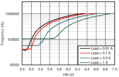
| VOUT = 5 V | FS = 1 MHz |
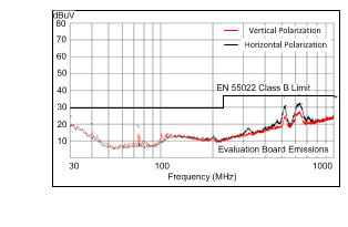
| VOUT = 5 V | FS = 500 kHz | IOUT = 1 A |
| Measured on the LM46001QPWPEVM with L = 27 µH, COUT = 66 µF, CFF = 33 pF. No input filter used. | ||
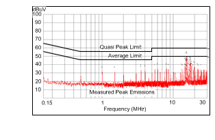
| VOUT = 5 V | FS = 500 kHz | IOUT = 1 A |
| Measured on the LM46001QPWPEVM with L = 27 µH, COUT = 66 µF, CFF = 33 pF. EVM input filter Lin = 1 µH Cd = 47 µF CIN4 = 68 µF | ||
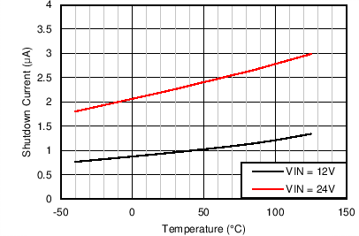

Junction Temperature

i.
Figure 32. Operating IQ vs VIN with BIAS Connected to VOUT
| VOUT = 3.3 V | FS = 500 kHz | IOUT = 0 A |