SNVSA46B June 2014 – January 2018 LM46001
PRODUCTION DATA.
- 1 Features
- 2 Applications
- 3 Description
- 4 Revision History
- 5 Pin Configuration and Functions
- 6 Specifications
-
7 Detailed Description
- 7.1 Overview
- 7.2 Functional Block Diagram
- 7.3
Feature Description
- 7.3.1 Fixed-Frequency, Peak-Current Mode Controlled Step-Down Regulator
- 7.3.2 Light Load Operation
- 7.3.3 Adjustable Output Voltage
- 7.3.4 Enable (ENABLE)
- 7.3.5 VCC, UVLO, and BIAS
- 7.3.6 Soft-Start and Voltage Tracking (SS/TRK)
- 7.3.7 Switching Frequency (RT) and Synchronization (SYNC)
- 7.3.8 Minimum ON-Time, Minimum OFF-Time and Frequency Foldback at Dropout Conditions
- 7.3.9 Internal Compensation and CFF
- 7.3.10 Bootstrap Voltage (CBOOT)
- 7.3.11 Power Good (PGOOD)
- 7.3.12 Overcurrent and Short-Circuit Protection
- 7.3.13 Thermal Shutdown
- 7.4 Device Functional Modes
-
8 Applications and Implementation
- 8.1 Application Information
- 8.2
Typical Applications
- 8.2.1 Design Requirements
- 8.2.2
Detailed Design Procedure
- 8.2.2.1 Custom Design With WEBENCH® Tools
- 8.2.2.2 Output Voltage Setpoint
- 8.2.2.3 Switching Frequency
- 8.2.2.4 Input Capacitors
- 8.2.2.5 Inductor Selection
- 8.2.2.6 Output Capacitor Selection
- 8.2.2.7 Feed-Forward Capacitor
- 8.2.2.8 Bootstrap Capacitors
- 8.2.2.9 VCC Capacitor
- 8.2.2.10 BIAS Capacitors
- 8.2.2.11 Soft-Start Capacitors
- 8.2.2.12 Undervoltage Lockout Setpoint
- 8.2.2.13 PGOOD
- 8.2.3 Application Curves
- 9 Power Supply Recommendations
- 10Layout
- 11Device and Documentation Support
- 12Mechanical, Packaging, and Orderable Information
Package Options
Mechanical Data (Package|Pins)
- PWP|16
Thermal pad, mechanical data (Package|Pins)
- PWP|16
Orderable Information
6.8 Typical Characteristics
Unless otherwise specified, VIN = 24 V, VOUT = 3.3 V, FS = 500 kHz, L = 18 µH, COUT = 100 µF, CFF = 33 pF. See Application Curves for bill of materials (BOM) for other VOUT and FS combinations.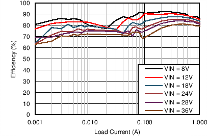
| VOUT = 3.3 V | FS = 500 kHz |
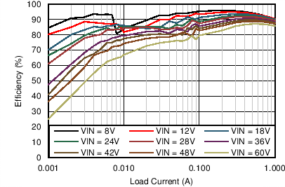
| VOUT = 5 V | FS = 200 kHz |
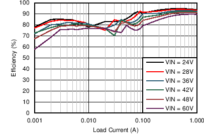
| VOUT = 12 V | FS = 500 kHz |
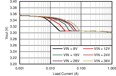
| VOUT = 3.3 V | FS = 500 kHz |
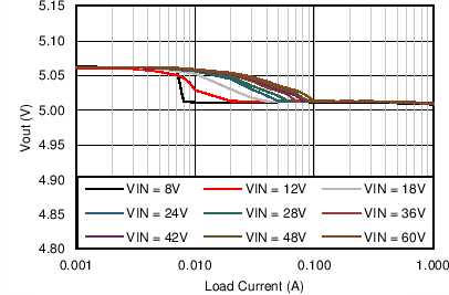
| VOUT = 5 V | FS = 200 kHz |
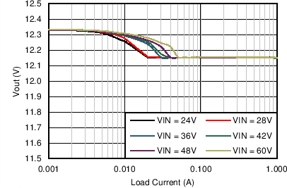
| VOUT = 12 V | FS = 500 kHz |
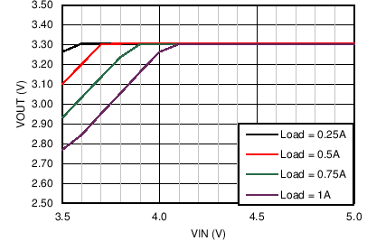
| VOUT = 3.3 V | FS = 500 kHz |
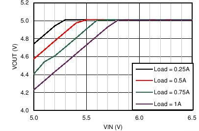
| VOUT = 5 V | FS = 200 kHz |
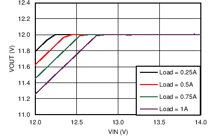
| VOUT = 12 V | FS = 500 kHz |

| VOUT = 3.3 V | FS = 500 kHz |

| VOUT = 3.3 V | FS = 500 kHz | IOUT = 1 A |
| Measured on the LM46001PWPEVM with default BOM. No input filter used. | ||

| VOUT = 3.3 V | FS = 500 kHz | IOUT = 1 A |
| Measured on LM46001PWPEVM with default BOM. EVM input filter: Lin = 1 µH Cd = 47 µF CIN4 = 68 µF | ||

Figure 25. High-Side and Low-side On Resistance vs Junction Temperature

Figure 27. Enable Threshold vs Junction Temperature

Figure 29. PGOOD Threshold vs Junction Temperature

| VIN = 24 V | VOUT = 3.3 V | FS = 500 kHz |
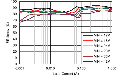
| VOUT = 5 V | FS = 500 kHz |

| VOUT = 5 V | FS = 1 MHz |
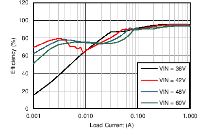
| VOUT = 24 V | FS = 500 kHz |
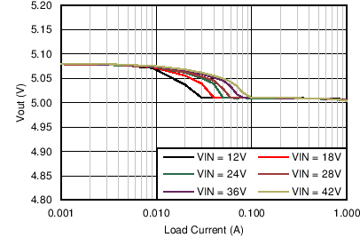
| VOUT = 5 V | FS = 500 kHz |
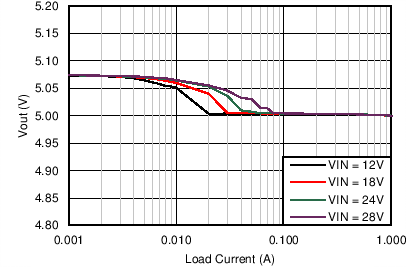
| VOUT = 5 V | FS = 1 MHz |
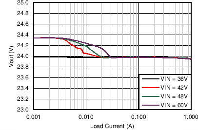
| VOUT = 24 V | FS = 500 kHz |
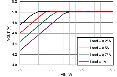
| VOUT = 5 V | FS = 500 kHz |
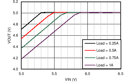
| VOUT = 5 V | FS = 1 MHz |
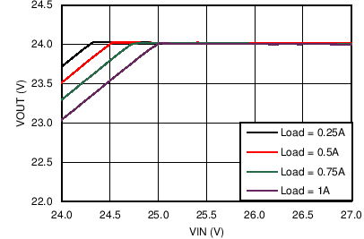
| VOUT = 24 V | FS = 500 kHz |

| VOUT = 5 V | FS = 1 MHz |
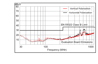
| VOUT = 5 V | FS = 500 kHz | IOUT = 1 A |
| Measured on the LM46001PWPEVM with L = 27 µH, COUT = 66 µF, CFF = 33 pF. No input filter used. | ||
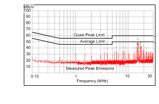
| VOUT = 5 V | FS = 500 kHz | IOUT = 1 A |
| Measured on LM46001PWPEVM with L = 27 µH, COUT = 66 µF, CFF = 33 pF. EVM input filter Lin = 1 µH Cd = 47 µF CIN4 = 68 µF | ||

Figure 26. Shutdown Current vs Junction Temperature

Figure 28. Enable Leakage Current vs
Junction Temperature

Figure 30. Feedback Voltage vs Junction Temperature

i.
Figure 32. Operating IQ vs VIN with BIAS Connected to VOUT| VOUT = 3.3 V | FS = 500 kHz | IOUT = 0 A |