SNVSA13C April   2014  – April 2019 LM46002

PRODUCTION DATA.  

  1. Features
  2. Applications
  3. Description
    1.     Device Images
      1.      Simplified Schematic
      2.      Radiated Emission Graph VIN = 24 V, VOUT = 3.3 V, FS= 500 kHz, IOUT = 2 A
  4. Revision History
  5. Pin Configuration and Functions
    1.     Pin Functions
  6. Specifications
    1. 6.1 Absolute Maximum Ratings
    2. 6.2 ESD Ratings
    3. 6.3 Recommended Operating Conditions
    4. 6.4 Thermal Information
    5. 6.5 Electrical Characteristics
    6. 6.6 Timing Requirements
    7. 6.7 Switching Characteristics
    8. 6.8 Typical Characteristics
  7. Detailed Description
    1. 7.1 Overview
    2. 7.2 Functional Block Diagram
    3. 7.3 Feature Description
      1. 7.3.1  Fixed-Frequency, Peak-Current-Mode-Controlled, Step-Down Regulator
      2. 7.3.2  Light Load Operation
      3. 7.3.3  Adjustable Output Voltage
      4. 7.3.4  Enable (ENABLE)
      5. 7.3.5  VCC, UVLO, and BIAS
      6. 7.3.6  Soft Start and Voltage Tracking (SS/TRK)
      7. 7.3.7  Switching Frequency (RT) and Synchronization (SYNC)
      8. 7.3.8  Minimum ON-Time, Minimum OFF-Time, and Frequency Foldback at Dropout Conditions
      9. 7.3.9  Internal Compensation and CFF
      10. 7.3.10 Bootstrap Voltage (BOOT)
      11. 7.3.11 Power Good (PGOOD)
      12. 7.3.12 Overcurrent and Short-Circuit Protection
      13. 7.3.13 Thermal Shutdown
    4. 7.4 Device Functional Modes
      1. 7.4.1 Shutdown Mode
      2. 7.4.2 Standby Mode
      3. 7.4.3 Active Mode
      4. 7.4.4 CCM Mode
      5. 7.4.5 Light Load Operation
      6. 7.4.6 Self-Bias Mode
  8. Applications and Implementation
    1. 8.1 Application Information
    2. 8.2 Typical Applications
      1. 8.2.1 Design Requirements
      2. 8.2.2 Detailed Design Procedure
        1. 8.2.2.1  Custom Design With WEBENCH® Tools
        2. 8.2.2.2  Output Voltage Setpoint
        3. 8.2.2.3  Switching Frequency
        4. 8.2.2.4  Input Capacitors
        5. 8.2.2.5  Inductor Selection
        6. 8.2.2.6  Output Capacitor Selection
        7. 8.2.2.7  Feed-Forward Capacitor
        8. 8.2.2.8  Bootstrap Capacitors
        9. 8.2.2.9  VCC Capacitor
        10. 8.2.2.10 BIAS Capacitors
        11. 8.2.2.11 Soft-Start Capacitors
        12. 8.2.2.12 Undervoltage Lockout Setpoint
        13. 8.2.2.13 PGOOD
      3. 8.2.3 Application Performance Curves
  9. Power Supply Recommendations
  10. 10Layout
    1. 10.1 Layout Guidelines
      1. 10.1.1 Compact Layout for EMI Reduction
      2. 10.1.2 Ground Plane and Thermal Considerations
      3. 10.1.3 Feedback Resistors
    2. 10.2 Layout Example
  11. 11Device and Documentation Support
    1. 11.1 Device Support
      1. 11.1.1 Development Support
        1. 11.1.1.1 Custom Design With WEBENCH® Tools
    2. 11.2 Receiving Notification of Documentation Updates
    3. 11.3 Community Resources
    4. 11.4 Trademarks
    5. 11.5 Electrostatic Discharge Caution
    6. 11.6 Glossary
  12. 12Mechanical, Packaging, and Orderable Information

Package Options

Mechanical Data (Package|Pins)
Thermal pad, mechanical data (Package|Pins)
Orderable Information

Typical Characteristics

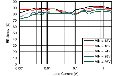
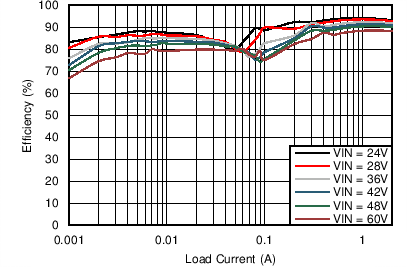
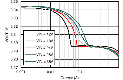
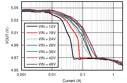
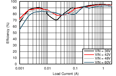
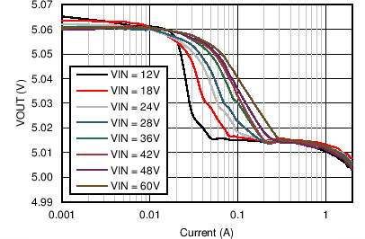
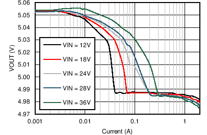
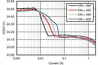
Unless otherwise specified, VIN = 24 V, VOUT = 3.3 V, FS = 500 kHz, L = 10 µH, COUT = 150 µF, CFF = 47 pF. Please refer to Application Performance Curves for Bill of Materials (BOM) for other VOUT and FS combinations.
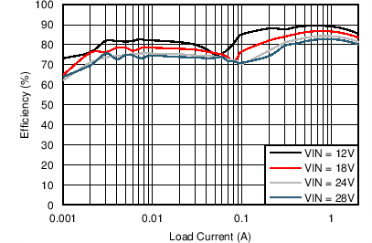
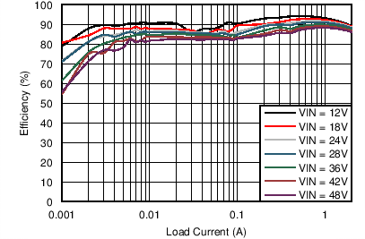
LM46002 C001_eff_3p3V_500kHz_snvsa13.png
VOUT = 3.3 V FS = 500 kHz
Figure 1. Efficiency
LM46002 C003_eff_5V_500kHz_snvsa13.png
VOUT = 5 V FS = 500 kHz
Figure 3. Efficiency
LM46002 C005_eff_12V_500kHz_snvsa13.png
VOUT = 12 V FS = 500 kHz
Figure 5. Efficiency
LM46002 C007_voutr_3p3V_500kHz_snvsa13.png
VOUT = 3.3 V FS = 500 kHz
Figure 7. VOUT Regulation
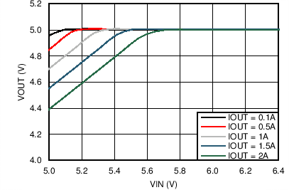
LM46002 C009_voutr_5V_500kHz_snvsa13.png
VOUT = 5 V FS = 500 kHz
Figure 9. VOUT Regulation
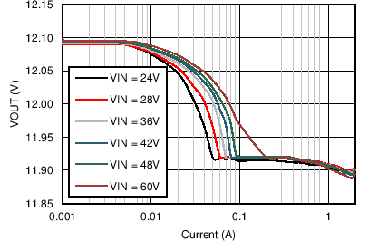
LM46002 C011_voutr_12V_500kHz_snvsa13.png
VOUT = 12 V FS = 500 kHz
Figure 11. VOUT Regulation
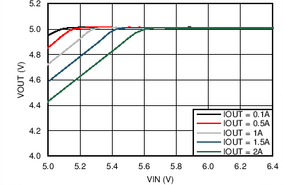
LM46002 C013_dropo_3p3V_500kHz_snvsa13.png
VOUT = 3.3 V FS = 500 kHz
Figure 13. Dropout Curve
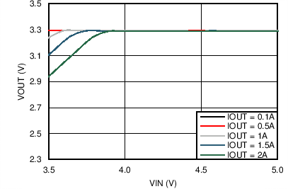
LM46002 C015_dropo_5V_500kHz_snvsa13.png
VOUT = 5 V FS = 500 kHz
Figure 15. Dropout Curve
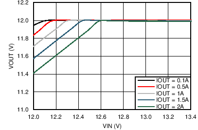
LM46002 C017_dropo_12V_500kHz_snvsa13.png
VOUT = 12 V FS = 500 kHz
Figure 17. Dropout Curve
LM46002 3p3V_500k_Fsw_Dropout.png
VOUT = 3.3 V FS = 500 kHz
Figure 19. Switching Frequency vs VIN in Dropout Operation
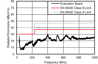
LM46002 EMI_Radiated_24V_5V_0p5MHz.png
VOUT = 3.3 V FS = 500 kHz IOUT = 2 A
Measured on the LM46002PWPEVM with default BOM. No input filter used.
Figure 21. Radiated EMI Curve
LM46002 EMI_Conducted_24V_3p3V_2A0p5MHz.png
VOUT = 3.3 V FS = 500 kHz IOUT = 2 A
Measured on the LM46002PWPEVM with default BOM. Input filter: Lin = 1 µH Cd = 47 µF CIN4 = 68 µF
Figure 23. Conducted EMI Curve
LM46002 RDSON_OverTemp.png
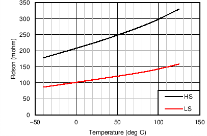
Figure 25. High-Side and Low-side On Resistance vs Junction Temperature
LM46002 EN_Threshold_OverTemp.png
Figure 27. Enable Threshold vs Junction Temperature
LM46002 PGOOD_Limits_OverTemp.png
Figure 29. PGOOD Threshold vs Junction Temperature
LM46002 3p3V_500k_PkValleyInductorCurr.png
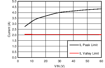
VOUT = 3.3 V FS = 500 kHz
Figure 31. Peak and Valley Current Limits vs VIN
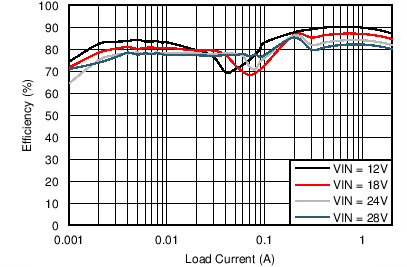
LM46002 C002_eff_5V_200kHz_snvsa13.png
VOUT = 5 V FS = 200 kHz
Figure 2. Efficiency
LM46002 C004_eff_5V_1MHz_snvsa13.png
VOUT = 5 V FS = 1 MHz
Figure 4. Efficiency
LM46002 C006_eff_24V_500kHz_snvsa13.png
VOUT = 24 V FS = 500 kHz
Figure 6. Efficiency
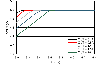
LM46002 C008_voutr_5V_200kHz_snvsa13.png
VOUT = 5 V FS = 200 kHz
Figure 8. VOUT Regulation
LM46002 C010_voutr_5V_1MHz_snvsa13.png
VOUT = 5 V FS = 1 MHz
Figure 10. VOUT Regulation
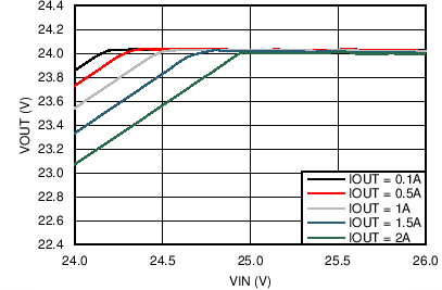
LM46002 C012_voutr_24V_500kHz_snvsa13.png
VOUT = 24 V FS = 500 kHz
Figure 12. VOUT Regulation
LM46002 C014_dropo_5V_200kHz_snvsa13.png
VOUT = 5 V FS = 200 kHz
Figure 14. Dropout Curve
LM46002 C016_dropo_5V_1MHz_snvsa13.png
VOUT = 5 V FS = 1 MHz
Figure 16. Dropout Curve
LM46002 C018_dropo_24V_500kHz_snvsa13.png
VOUT = 24 V FS = 500 kHz
Figure 18. Dropout Curve
LM46002 5V_1M_Fsw_Dropout.png
VOUT = 5 V FS = 1 MHz
Figure 20. Switching Frequency vs VIN in Dropout Operation
LM46002 EMI_Radiated_12V_3p3V_2A_1MHz.png
VOUT = 5 V FS = 1 MHz IOUT = 2 A
Measured on the LM46002PWPEVM with L = 6.8 µH, COUT = 47 µF, CFF = 47 pF. No input filter used.
Figure 22. Radiated EMI Curve
LM46002 EMI_Conducted_24V_V_2A_1MHz.png
VOUT = 5 V FS = 1 MHz IOUT = 2 A
Measured on the LM46002PWPEVM with L = 6.8 µH, COUT = 47 µF, CFF = 47 pF. Input filter Lin = 1 µH Cd = 47 µF CIN4 = 68 µF
Figure 24. Conducted EMI Curve
LM46002 Shutdown_Current_OverTemp.png
Figure 26. Shutdown Current vs Junction Temperature
LM46002 EN_Leakage_Current_OverTemp.png
Figure 28. Enable Leakage Current vs
Junction Temperature
LM46002 1V_200k_VFB_Temperature.png
Figure 30. Feedback Voltage vs Junction Temperature
LM46002 3p3V_500k_Iq.png
VOUT = 3.3 V FS = 500 kHz IOUT = 0 A
EN pin is connected to external 5 V rail
Figure 32. Operation IQ vs VIN with BIAS Connected to VOUT