SNAS416K July 2007 – November 2019 LM48511
PRODUCTION DATA.
- 1 Features
- 2 Applications
- 3 Description
- 4 Revision History
- 5 Pin Configuration and Functions
- 6 Specifications
- 7 Detailed Description
-
8 Application and Implementation
- 8.1 Application Information
- 8.2
Typical Application
- 8.2.1 Design Requirements
- 8.2.2
Detailed Design Procedure
- 8.2.2.1 Proper Selection of External Components
- 8.2.2.2 Power Supply Bypassing
- 8.2.2.3 Audio Amplifier Gain Setting Resistor Selection
- 8.2.2.4 Audio Amplifier Input Capacitor Selection
- 8.2.2.5 Selecting Regulator Output Capacitor
- 8.2.2.6 Selecting Regulating Bypass Capacitor
- 8.2.2.7 Selecting the Soft-Start (CSS) Capacitor
- 8.2.2.8 Selecting Diode (D1)
- 8.2.2.9 Duty Cycle
- 8.2.2.10 Selecting Inductor Value
- 8.2.2.11 Inductor Supplies
- 8.2.2.12 Setting the Regulator Output Voltage (PV1)
- 8.2.2.13 Discontinuous and Continuous Operation
- 8.2.2.14 ISW Feed-Forward Compensation for Boost Converter
- 8.2.2.15 Calculating Regulator Output Current
- 8.2.2.16 Design Parameters VSW and ISW
- 8.2.3 Application Curve
- 9 Power Supply Recommendations
- 10Layout
- 11Device and Documentation Support
- 12Mechanical, Packaging, and Orderable Information
Package Options
Mechanical Data (Package|Pins)
- NHZ|24
Thermal pad, mechanical data (Package|Pins)
Orderable Information
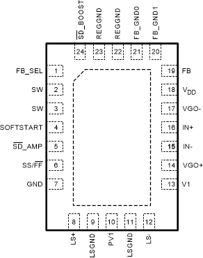
5 Pin Configuration and Functions
NHZ Package
24-Pin WQFN
Top View

Pin Functions
| PIN | I/O | DESCRIPTION | |
|---|---|---|---|
| NAME | NO. | ||
| DAP | – | — | To be soldered to board for enhanced thermal dissipation. Connect to GND plane. |
| FB | 19 | — | Regulator feedback input
Connect FB to an external resistive voltage divider to set the boost output voltage. |
| FB_GND0 | 21 | — | Ground return for R3, R1 resistor divider |
| FB_GND1 | 20 | — | Ground return for R3, R2 resistor divider |
| FB_SEL | 1 | I | Regulator feedback select
Connect to VDD to select feedback network connected to FB_GND1. Connect to GND to select feedback network connected to FB_GND0. |
| GND | 7 | — | Signal ground |
| IN– | 15 | I | Amplifier inverting input |
| IN+ | 16 | I | Amplifier noninverting input |
| LS+ | 8 | O | Amplifier noninverting output |
| LS– | 12 | O | Amplifier inverting output |
| LSGND | 9, 11 | — | Amplifier H-Bridge ground |
| PV1 | 10 | — | Amplifier H-Bridge power supply
Connect to V1. |
| REGGND | 22, 23 | — | Power ground (booster) |
| SD_AMP | 5 | I | Amplifier active-low shutdown
Connect to VDD for normal operation. Connect to GND to disable amplifier. |
| SD_BOOST | 24 | I | Regulator active-low shutdown.
Connect to VDD for normal operation. Connect to GND to disable regulator. |
| SOFT-START | 4 | — | Soft-start capacitor |
| SS/FF | 6 | I | Modulation mode select.
Connect to VDD for spread spectrum mode (SS). Connect to GND for fixed frequency mode (FF). |
| SW | 2, 3 | — | Drain of the internal FET switch |
| V1 | 13 | — | Amplifier supply voltage
Connect to PV1 |
| VDD | 18 | — | Power supply |
| VG0+ | 14 | O | Amplifier noninverting gain output |
| VG0– | 17 | O | Amplifier inverting gain output |