SNAS513F August 2011 – November 2015 LM48560
PRODUCTION DATA.
- 1 Features
- 2 Applications
- 3 Description
- 4 Revision History
- 5 Pin Configuration and Functions
- 6 Specifications
- 7 Parameter Measurement Information
- 8 Detailed Description
- 9 Application and Implementation
- 10Power Supply Recommendations
- 11Layout
- 12Device and Documentation Support
- 13Mechanical, Packaging, and Orderable Information
Package Options
Mechanical Data (Package|Pins)
- YZR|16
Thermal pad, mechanical data (Package|Pins)
Orderable Information
8 Detailed Description
8.1 Overview
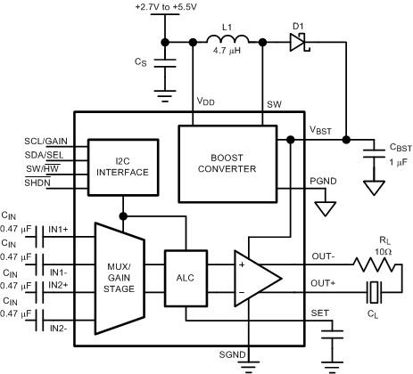
The LM48560 device is a fully differential Class H driver for ceramic speakers and piezo actuators. The integrated, high efficiency boost converter dynamically adjusts the amplifier’s supply voltage based on the output signal to maintain sufficient headroom while improving efficiency. The LM48560 device’s Class H architecture offers significant power savings compared to conventional Class AB drivers. The LM48560 features two fully differential inputs with separate gain settings, and a selectable control interface. In software control mode, the gain control and device modes are configured through the I2C interface. In hardware control mode, the gain and input mux are configured through a pair of logic inputs.
8.2 Functional Block Diagram

8.3 Feature Description
8.3.1 General Amplifier Function
The LM48560 device is a fully differential, Class H piezo driver for ceramic speakers and haptic actuators. The integrated, high efficiency boost converter dynamically adjusts the amplifier’s supply voltage based on the output signal, increasing headroom and improving efficiency compared to a conventional Class AB driver. The fully differential amplifier takes advantage of the increased headroom and bridge-tied load (BTL) architecture, delivering significantly more voltage than a single-ended amplifier.
8.3.2 Class H Operation
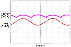
Class H is a modification of another amplifier class (typically Class B or Class AB) to increase efficiency and reduce power dissipation. To decrease power dissipation, Class H uses a tracking power supply that monitors the output signal and adjusts the supply accordingly. When the amplifier output is below 3VP-P, the nominal boost voltage is 6 V. As the amplifier output increases above 3 VP-P, the boost voltage tracks the amplifier output as shown in Figure 24. When the amplifier output falls below 3 VP-P, the boost converter returns to its nominal output voltage. Power dissipation is greatly reduced compared to conventional Class AB drivers.
 Figure 24. Class H Operation
8.3.3 Differential Amplifier Explanation
The LM48560 device features a fully differential amplifier. A differential amplifier amplifies the difference between the two input signals. A major benefit of the fully differential amplifier is the improved common mode rejection ratio (CMRR) over single ended input amplifiers. The increased CMRR of the differential amplifier reduces sensitivity to ground offset related noise injection, especially important in noisy systems.
8.3.4 Automatic Level Control (ALC)
The ALC is available in software mode only, and only in boosted mode. In hardware mode ALC is always disabled. The ALC limits the peak output voltage to the programmed value. Consequently, it limits the peak boost voltage, as this is derived from the output voltage. The ALC is continuous, in that it provides a continuous adjustment of the voltage gain to limit the output voltage to the programmed value. The available gain adjustment range is typically 8 dB. When the input amplitude is further increased beyond the ALC attenuation range, the output will again increase. This is illustrated in the Typical Performance Graphs, as seen on the 14 VPP plot in the Input voltage vs Output Voltage curve. The attack and decay of the ALC is programmed by software and works in conjunction with the external capacitor CSET. Typically CSET is 0.1 μF, although it can be changed from 0.1 μF to 4.7 μF to select other ranges of attack and decay time.
8.3.5 Attack Time
Attack time (tATK) is the time it takes for the gain to be reduced by 6 dB once the audio signal exceeds the ALC threshold. Fast attack times allow the ALC to react quickly and prevent transients such as symbol crashes from being distorted. However, fast attack times can lead to volume pumping, where the gain reduction and release becomes noticeable, as the ALC cycles quickly. Slower attack times cause the ALC to ignore the fast transients, and instead act upon longer, louder passages. Selecting an attack time that is too slow can lead to increased distortion in the case of the No Clip function, and possible output overload conditions in the case of the Voltage limiter. The attack time is set by a combination of the value of CSET and the attack time coefficient as given by Equation 1:
Where αATK is the attack time coefficient (Table 1) set by bits B4:B3 in the Voltage Limit Control Register. The attack time coefficient allows the user to set a nominal attack time. The internal 20 kΩ resistor is subject to temperature change, and it has tolerance between –11% to +20%.
Table 1. Attack Time Coefficient
| B4 | B3 | αATK |
|---|---|---|
| 0 | 0 | 2.4 |
| 0 | 1 | 1.7 |
| 1 | 0 | 1.3 |
| 1 | 1 | 0.9 |
8.3.6 Release Time
Release time (tRL) is the time it takes for the gain to return from 6 dB to its normal level once the audio signal returns below the ALC threshold. A fast release time allows the ALC to react quickly to transients, preserving the original dynamics of the audio source. However, similar to a fast attack time, a fast release time contributes to volume pumping. A slow release time reduces the effect of volume pumping. The release time is set by a combination of the value of CSET and release time coefficient as given by Equation 2:
where αRL is the release time coefficient (Table 2) set by bits B6:B5 in the No Clip Control Register. The release time coefficient allows the user to set a nominal release time. The internal 20 MΩ is subject to temperature change, and it has tolerance between -11% to +20%.
Table 2. Release Time Coefficient
| B6 | B5 | αRL |
|---|---|---|
| 0 | 0 | 4 |
| 0 | 1 | 5.3 |
| 1 | 0 | 9.5 |
| 1 | 1 | 11.8 |
8.3.7 Boost Converter
The LM48560 device features an integrated boost converter with a dynamic output control. The device monitors the output signal of the amplifier, and adjusts the output voltage of the boost converter to maintain sufficient headroom while improving efficiency.
8.3.8 Gain Setting
The LM48560 device features four internally configured gain settings 0 db, 6 dB, and 30 dB. The device gain is selected through a single pin (GAIN). The gain settings are shown in Table 3.
Table 3. Gain Setting
| GAIN | GAIN SETTING IN1 |
GAIN SETTING IN2 |
|---|---|---|
| 0 | 0 dB | 24 dB |
| 1 | 6 dB | 30 dB |
8.3.9 Shutdown Function
The LM48560 device features a low current shutdown mode. Set SD = GND to disable the amplifier and boost converter and reduce supply current to 0.01 µA.
8.4 Device Functional Modes
8.4.1 Software or Hardware Mode
Device operation in hardware or software mode is determined by the state of the SW/HW pin. Connect SW/HW to ground for hardware mode, and connect to VDD for software mode.
| SW/HW | SDA/SEL | SCL/GAIN | MODE |
|---|---|---|---|
| 0 | 0 (Boost Disabled) |
0 | IN1, Av = 0 |
| 1 | IN1, Av = 6 | ||
| 1 (Boost Enabled) |
0 | IN2, Av = 24 | |
| 1 | IN2, Av = 30 | ||
| 1 | SDA | SCL | I2C Mode |
8.4.2 Single-Ended Input Configuration
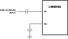
The LM48560 device is compatible with single-ended sources. When configured for single-ended inputs, input capacitors must be used to block and DC component at the input of the device. Figure 25 shows the typical single-ended applications circuit.
 Figure 25. Single-Ended Input Configuration
8.5 Programming
8.5.1 Read/Write I2C Compatible Interface
The LM48560 device is controlled through an I2C compatible serial interface that consists of a serial data line (SDA) and a serial clock (SCL). The clock line is uni-directional. The data line is bi-directional (open drain). The LM48560 device and the master can communicate at clock rates up to 400 kHz. Figure 1 shows the I2C interface timing diagram. Data on the SDA line must be stable during the HIGH period of SCL. The LM48560 device is a transmit/receive slave-only device, reliant upon the master to generate the SCL signal. Each transmission sequence is framed by a START condition and a STOP condition Figure 2. Each data word, device address and data, transmitted over the bus is 8 bits long and is always followed by an acknowledge pulse Figure 26. The LM48560 device address is 1101111.
8.5.2 Write Sequence
The example write sequence is shown in Figure 26. The START signal, the transition of SDA from HIGH to LOW while SDA is HIGH, is generated, altering all devices on the bus that a device address is being written to the bus.
The 7-bit device address is written to the bus, most significant bit (MSB) first, followed by the R/W bit (R/W = 0 indicating the master is writing to the LM48560 device). The data is latched in on the rising edge of the clock. Each address bit must be stable while SDA is HIGH. After the R/W bit is transmitted, the master device releases SDA, during which time, an acknowledge clock pulse is generated by the slave device. If the LM48560 device receives the correct address, the device pulls the SDA line low, generating and acknowledge bit (ACK).
Once the master device registers the ACK bit, the 8-bit register address word is sent, MSB first. Each data bit should be stable while SCL is HIGH. After the 8-bit register address is sent, the LM48560 device sends another ACK bit. Upon receipt of the acknowledge, the 8-bit register data is sent, MSB first. The register data word is followed by an ACK, upon receipt of which, the master issues a STOP bit, allowing SDA to go high while SDA is high.
 Figure 26. Example I2C Write Cycle
8.5.3 Read Sequence
The example read sequence is shown in Figure 27. The START signal, the transition of SDA from HIGH to LOW while SDA is HIGH, is generated, altering all devices on the bus that a device address is being written to the bus.
The 7-bit device address is written to the bus, followed by the R/W = 1 (R/W = 1 indicating the master wants to read data from the LM48560 device). After the R/W bit is transmitted, the master device releases SDA, during which time, an acknowledge clock pulse is generated by the slave device. If the LM48560 device receives the correct address, the device pulls the SDA line low, generating and acknowledge bit (ACK). Once the master device registers the ACK bit, the 8-bit register address word is sent, MSB first, followed by an ACK and selected register data from the LM48560 device. The register data is sent MSB first. Following the acknowledgment of the register data word [7:0], the master issues a STOP bit, allowing SDA to go high while SDA is high.
 Figure 27. Example I2C Read Cycle
Table 4. Device Address
| B7 | B6 | B5 | B4 | B3 | B2 | B1 | B0 (R/W) | |
|---|---|---|---|---|---|---|---|---|
| Device Address | 1 | 1 | 0 | 1 | 1 | 1 | 1 | 0 |
Table 5. Mode Selection
| SW/HW | SDA/SEL | SCL/GAIN | MODE |
|---|---|---|---|
| 0 | 0 (Boost Disabled) |
0 | IN1, AV = 0 |
| 1 | IN1, AV = 6 | ||
| 1 (Boost Enabled) |
0 | IN2, AV = 24 | |
| 1 | IN2, AV = 30 | ||
| 1 | X | X | I2C Mode |
8.6 Register Maps
Table 6. I2C Control Registers
| REGISTER ADDRESS |
Register Name |
B7 | B6 | B5 | B4 | B3 | B2 | B1 | B0 |
|---|---|---|---|---|---|---|---|---|---|
| 0x00h | SHUTDOWN CONTROL | X | X | X | X | TURN _ON |
IN_SEL | BOOST _EN |
SHDN |
| 0x01h | NO CLIP CONTROL | X | RLT1 | RLT0 | ATK1 | ATK0 | PLEV2 | PLEV1 | PLEV0 |
| 0x02h | GAIN CONTROL | X | X | X | X | X | X | GAIN1 | GAIN0 |
| 0x03h | TEST MODE | X | X | X | X | X | X | X | X |
Table 7. Shutdown Control Register
| BIT | NAME | VALUE | DESCRIPTION |
|---|---|---|---|
| B7:B4 | UNUSED | X | Unused, set to 0 |
| B3 | TURN_ON | 0 | Normal turn on time, tWU = 15 ms |
| 1 | Fast turn on time, tWU = 5 ms | ||
| B2 | IN_SEL | 0 | Input 1 selected |
| 1 | Input 2 selected | ||
| B1 | BOOST_EN | 0 | Boost disabled |
| 1 | Boost enabled | ||
| B0 | SHDN | 0 | Device shutdown |
| 1 | Device enabled |
Table 8. No Clip Control Register
| BIT | NAME | VALUE | DESCRIPTION | ||
|---|---|---|---|---|---|
| B7 | UNUSED | X | Unused, set to 0 | ||
| B6:B5 | RLT1 (B6) RLT0 (B5) |
B6 | B5 | Sets Release Time based on CSET. See Release Time section. |
|
| 0 | 0 | TR = 0.5 s | |||
| 0 | 1 | TR = 0.38 s | |||
| 1 | 0 | TR = 0.21 s | |||
| 1 | 1 | TR = 0.17 s | |||
| B4:B3 | ATK1 (B4) ATK0 (B3) |
B4 | B3 | Sets Attack Time based on CSET. See Attack Time section. |
|
| 0 | 0 | TA = 0.83 ms | |||
| 0 | 1 | TA = 1.2 ms | |||
| 1 | 0 | TA = 1.5 ms | |||
| 1 | 1 | TA = 2.2 ms | |||
| B2:B0 | PLEV2 (B2) PLEV1 (B1) PLEV0 (B0) |
B2 | B1 | B0 | Sets output voltage limit level. |
| 0 | 0 | 0 | Voltage Limit disabled | ||
| 0 | 0 | 1 | VTH(VLIM) = 14 VP-P | ||
| 0 | 1 | 0 | VTH(VLIM) = 17 VP-P | ||
| 0 | 1 | 1 | VTH(VLIM) = 20 VP-P | ||
| 1 | 0 | 0 | VTH(VLIM) = 22 VP-P | ||
| 1 | 0 | 1 | VTH(VLIM) = 25 VP-P | ||
| 1 | 1 | 0 | VTH(VLIM) = 28 VP-P | ||
| 1 | 1 | 1 | Voltage Limit disabled | ||
Table 9. Gain Control Register
| BIT | NAME | VALUE | DESCRIPTION | |
|---|---|---|---|---|
| B7:B2 | UNUSED | X | Unused, set to 0 | |
| B1:B0 | GAIN1(B1) GAIN0 (B0) |
B1 | B0 | Sets amplifier gain. Boost disabled (BOOST_EN = 0) |
| 0 | 0 | 0 dB | ||
| 0 | 1 | 6 dB | ||
| 1 | 0 | 12 dB | ||
| 1 | 1 | 18 dB | ||
| B1:B0 | GAIN1(B1) GAIN0 (B0) |
B1 | B0 | Sets amplifier gain. Boost enabled (BOOST_EN = 1) |
| 0 | 0 | 21 dB | ||
| 0 | 1 | 24 dB | ||
| 1 | 0 | 27 dB | ||
| 1 | 1 | 30 dB | ||