SNIS118G July 1999 – January 2017 LM50 , LM50-Q1
PRODUCTION DATA.
- 1 Features
- 2 Applications
- 3 Description
- 4 Revision History
- 5 Pin Configuration and Functions
- 6 Specifications
- 7 Detailed Description
- 8 Application and Implementation
- 9 Power Supply Recommendations
- 10Layout
- 11Device and Documentation Support
- 12Mechanical, Packaging, and Orderable Information
Refer to the PDF data sheet for device specific package drawings
Mechanical Data (Package|Pins)
- DBZ|3
Thermal pad, mechanical data (Package|Pins)
8 Application and Implementation
NOTE
Information in the following applications sections is not part of the TI component specification, and TI does not warrant its accuracy or completeness. TI’s customers are responsible for determining suitability of components for their purposes. Customers should validate and test their design implementation to confirm system functionality.
8.1 Application Information
The LM50 and LM50-Q1 have a wide supply range and a 10 mV/°C output slope with a 500-mV DC offset. Therefore, it can be easily applied in many temperature-sensing applications where a single supply is required for positive and negative temperatures.
8.2 Typical Application
8.2.1 Full-Range Centigrade Temperature Sensor
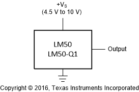
 Figure 12. Full-Range Centigrade Temperature Sensor Diagram(–40°C to 125°C)
8.2.1.1 Design Requirements
For this design example, use the parameters listed in Table 1 as the input parameters.
Table 1. Design Parameters
| PARAMETER | VALUE |
|---|---|
| Power supply voltage | ±3°C (maximum) |
| Output impedance | ±4°C (maximum) |
| Accuracy at 25°C | 10 mV/°C |
| Accuracy over –40°C to 125°C | 4.5 V to 10 V |
| Temperature slope | 4 kΩ (maximum) |
8.2.1.2 Detailed Design Procedure
The LM50 and LM50-Q1 are simple temperature sensors that provides an analog output. Therefore design requirements related to layout are more important than other requirements. See Layout for more information.
8.2.1.2.1 Capacitive Loads
The LM50 and LM50-Q1 handle capacitive loading very well. Without any special precautions, the LM50 and LM50-Q1 can drive any capacitive load. The device has a nominal 2-kΩ output impedance (shown in Functional Block Diagram). The temperature coefficient of the output resistors is around 1300 ppm/°C. Taking into account this temperature coefficient and the initial tolerance of the resistors the output impedance of the device will not exceed 4 kΩ. In an extremely noisy environment it may be necessary to add some filtering to minimize noise pickup. TI recommends adding a 0.1-µF capacitor between +VS and GND to bypass the power supply voltage, as shown in Figure 14. It may also be necessary to add a capacitor from VOUT to ground. A 1-µF output capacitor with the 4-kΩ output impedance will form a 40-Hz low-pass filter. Since the thermal time constant of the LM50 and LM50-Q1 is much slower than the 25-ms time constant formed by the RC, the overall response time of the device will not be significantly affected. For much larger capacitors this additional time lag will increase the overall response time of the LM50 and LM50-Q1.
 Figure 13. LM50 and LM50-Q1 No Decoupling Required
for Capacitive Load
 Figure 14. LM50C and LM50-Q1 with Filter for Noisy Environment
8.2.1.3 Application Curve
 Figure 15. Output Transfer Function
8.3 System Examples
Figure 16 to Figure 18 show application circuit examples using the LM50 or LM50-Q1 devices. Customers must fully validate and test any circuit before implementing a design based on an example in this section. Unless otherwise noted, the design procedures in Full-Range Centigrade Temperature Sensor are applicable.
 Figure 16. Centigrade Thermostat or Fan Controller

