SNIS118G July 1999 – January 2017 LM50 , LM50-Q1
PRODUCTION DATA.
- 1 Features
- 2 Applications
- 3 Description
- 4 Revision History
- 5 Pin Configuration and Functions
- 6 Specifications
- 7 Detailed Description
- 8 Application and Implementation
- 9 Power Supply Recommendations
- 10Layout
- 11Device and Documentation Support
- 12Mechanical, Packaging, and Orderable Information
Refer to the PDF data sheet for device specific package drawings
Mechanical Data (Package|Pins)
- DBZ|3
Thermal pad, mechanical data (Package|Pins)
6 Specifications
6.1 Absolute Maximum Ratings
over operating free-air temperature range (unless otherwise noted)(1)| MIN | MAX | UNIT | |
|---|---|---|---|
| Supply voltage | –0.2 | 12 | V |
| Output voltage | –1 | +VS + 0.6 | V |
| Output current | 10 | mA | |
| Maximum junction temperature, TJ | 150 | °C | |
| Storage temperature, Tstg | –65 | 150 | °C |
(1) Stresses beyond those listed under Absolute Maximum Ratings may cause permanent damage to the device. These are stress ratings only, which do not imply functional operation of the device at these or any other conditions beyond those indicated under Recommended Operating Conditions. Exposure to absolute-maximum-rated conditions for extended periods may affect device reliability.
6.2 ESD Ratings
| VALUE | UNIT | |||
|---|---|---|---|---|
| LM50 | ||||
| V(ESD) | Electrostatic discharge | Human body model (HBM)(1) | ±2000 | V |
| Charged-device model (CDM) | ±750 | |||
| Machine model(1) | ±250 | |||
| LM50-Q1 | ||||
| V(ESD) | Electrostatic discharge | Human-body model (HBM), per AEC Q100-002(2) | ±2000 | V |
| Charged-device model (CDM), per AEC Q100-011 | ±750 | |||
(1) The human body model is a 100-pF capacitor discharged through a 1.5-kΩ resistor into each pin. Machine model is a 200-pF capacitor discharged directly into each pin.
(2) AEC Q100-002 indicates that HBM stressing shall be in accordance with the ANSI/ESDA/JEDEC JS-001 specification.
6.3 Recommended Operating Conditions(1)
| MIN | MAX | UNIT | |||
|---|---|---|---|---|---|
| +VS | Supply voltage | 4.5 | 10 | V | |
| TMIN, TMAX | Specified temperature | LM50C, LM50-Q1 | –40 | 125 | °C |
| LM50B | –25 | 100 | |||
| Operating temperature | –40 | 150 | °C | ||
(1) Soldering process must comply with the Reflow Temperature Profile specifications. Reflow temperature profiles are different for lead-free and non-lead-free packages. Refer to www.ti.com/packaging.
6.4 Thermal Information
| THERMAL METRIC(1) | LM50, LM50-Q1 | UNIT | |
|---|---|---|---|
| DBZ (SOT-23) | |||
| 3 PINS | |||
| RθJA | Junction-to-ambient thermal resistance | 291.9 | °C/W |
| RθJC(top) | Junction-to-case (top) thermal resistance | 114.3 | °C/W |
| RθJB | Junction-to-board thermal resistance | 62.3 | °C/W |
| φJT | Junction-to-top characterization parameter | 7.4 | °C/W |
| φJB | Junction-to-board characterization parameter | 61 | °C/W |
(1) For more information about traditional and new thermal metrics, see the Semiconductor and IC Package Thermal Metrics application report.
6.5 Electrical Characteristics: LM50B
+VS = 5 V (DC) and ILOAD = 0.5 µA, in the circuit of Figure 12, TA = TJ = 25°C (unless otherwise noted)(1)| PARAMETER | TEST CONDITIONS | MIN | TYP | MAX | UNIT |
|---|---|---|---|---|---|
| Accuracy(2) | TA = 25°C | –2 | 2 | °C | |
| TA = TMAX | –3 | 3 | °C | ||
| TA = TMIN | –3.5 | 3 | °C | ||
| Nonlinearity(3) | TA = TJ = TMIN to TMAX | –0.8 | 0.8 | °C | |
| Sensor gain (average slope) | TA = TJ = TMIN to TMAX | 9.7 | 10.3 | mV/°C | |
| Output resistance | TA = TJ = TMIN to TMAX | 2000 | 4000 | Ω | |
| Line regulation(4) | +VS = 4.5 V to 10 V, TA = TJ = TMIN to TMAX | –1.2 | 1.2 | mV/V | |
| Quiescent current(5) | +VS = 4.5 V to 10 V, TA = TJ = TMIN to TMAX | 180 | µA | ||
| Change of quiescent current | +VS = 4.5 V to 10 V, TA = TJ = TMIN to TMAX | 2 | µA | ||
| Temperature coefficient of quiescent current | TA = TJ = TMIN to TMAX | 1 | µA/°C | ||
| Long term stability(6) | TJ = 125°C, for 1000 hours | ±0.08 | °C |
(1) Limits are specified to TI's AOQL (Average Outgoing Quality Level).
(2) Accuracy is defined as the error between the output voltage and 10 mv/°C multiplied by the device's case temperature plus 500 mV, at specified conditions of voltage, current, and temperature (expressed in °C).
(3) Nonlinearity is defined as the deviation of the output-voltage-versus-temperature curve from the best-fit straight line, over the device's rated temperature range.
(4) Regulation is measured at constant junction temperature, using pulse testing with a low duty cycle. Changes in output due to heating effects can be computed by multiplying the internal dissipation by the thermal resistance.
(5) Quiescent current is defined in the circuit of Figure 12.
(6) For best long-term stability, any precision circuit will give best results if the unit is aged at a warm temperature, and/or temperature cycled for at least 46 hours before long-term life test begins. This is especially true when a small (Surface-Mount) part is wave-soldered; allow time for stress relaxation to occur. The majority of the drift occurs in the first 1000 hours at elevated temperatures. The drift after 1000 hours does not continue at the first 1000 hour rate.
6.6 Electrical Characteristics: LM50C and LM50-Q1
+VS = 5 V (DC) and ILOAD = 0.5 µA, in the circuit of Figure 12. TA = TJ = 25°C, unless otherwise noted.(1)| PARAMETER | TEST CONDITIONS | MIN | TYP | MAX | UNIT |
|---|---|---|---|---|---|
| Accuracy(1) | TA = 25°C | –3 | 3 | °C | |
| TA = TMAX | –4 | 4 | °C | ||
| TA = TMIN | –4 | 4 | °C | ||
| Nonlinearity(2) | TA = TJ = TMIN to TMAX | –0.8 | 0.8 | °C | |
| Sensor gain(average slope) | TA = TJ = TMIN to TMAX | 9.7 | 10.3 | mV/°C | |
| Output resistance | TA = TJ = TMIN to TMAX | 2000 | 4000 | Ω | |
| Line regulation(3) | +VS = 4.5 V to 10 V, TA = TJ = TMIN to TMAX | –1.2 | 1.2 | mV/V | |
| Quiescent current(4) | +VS = 4.5 V to 10 V, TA = TJ = TMIN to TMAX | 180 | µA | ||
| Change of quiescent current | +VS = 4.5 V to 10 V, TA = TJ = TMIN to TMAX | 2 | µA | ||
| Temperature coefficient of quiescent current | TA = TJ = TMIN to TMAX | 2 | µA/°C | ||
| Long term stability(5) | TJ = 125°C, for 1000 hours | ±0.08 | °C |
(1) Accuracy is defined as the error between the output voltage and 10 mv/°C multiplied by the device's case temperature plus 500 mV, at specified conditions of voltage, current, and temperature (expressed in °C).
(2) Nonlinearity is defined as the deviation of the output-voltage-versus-temperature curve from the best-fit straight line, over the device's rated temperature range.
(3) Regulation is measured at constant junction temperature, using pulse testing with a low duty cycle. Changes in output due to heating effects can be computed by multiplying the internal dissipation by the thermal resistance.
(4) Quiescent current is defined in the circuit of Figure 12.
(5) For best long-term stability, any precision circuit will give best results if the unit is aged at a warm temperature, and/or temperature cycled for at least 46 hours before long-term life test begins. This is especially true when a small (Surface-Mount) part is wave-soldered; allow time for stress relaxation to occur. The majority of the drift occurs in the first 1000 hours at elevated temperatures. The drift after 1000 hours does not continue at the first 1000 hour rate.
6.7 Typical Characteristics
To generate these curves the device was mounted to a printed circuit board as shown in Figure 20.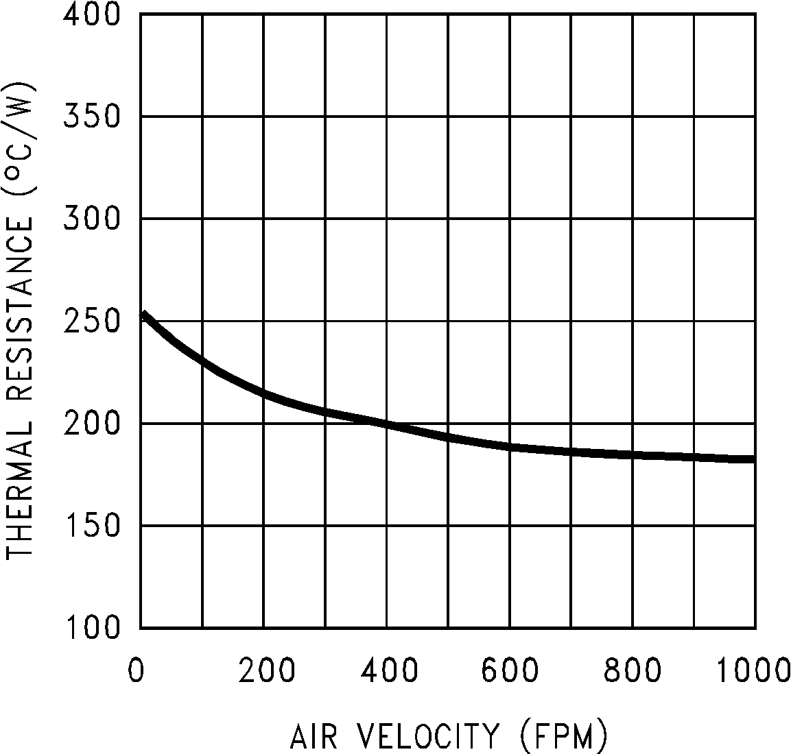 Figure 1. Junction-to-Ambient Thermal Resistance
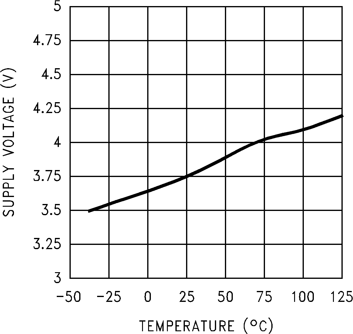 Figure 5. Start-Up Voltage vs Temperature
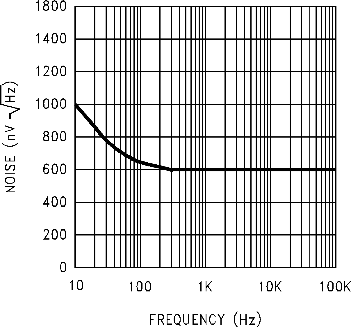 Figure 9. Noise Voltage
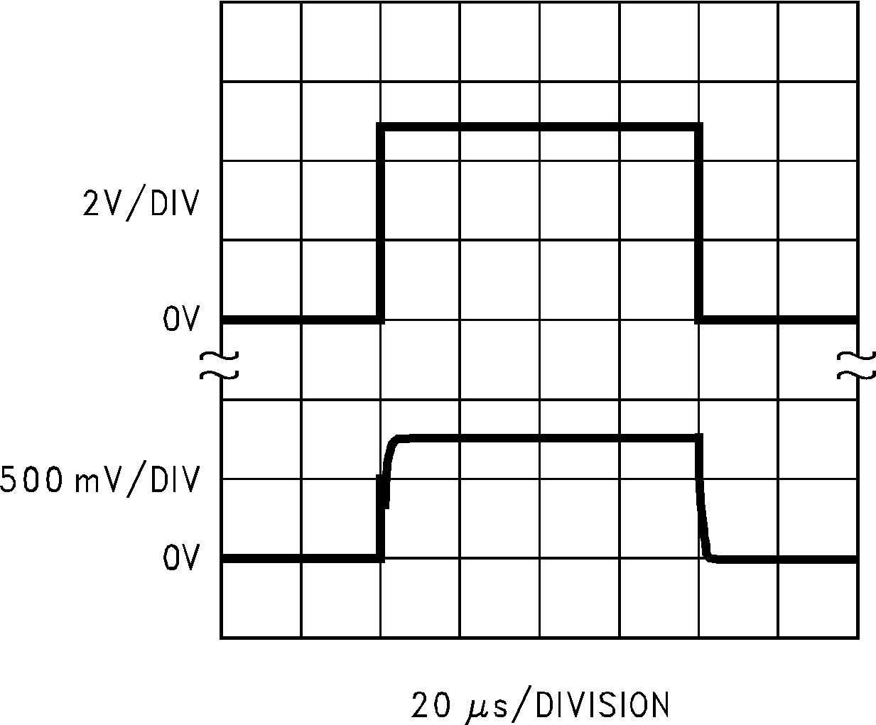 Figure 11. Start-Up Response
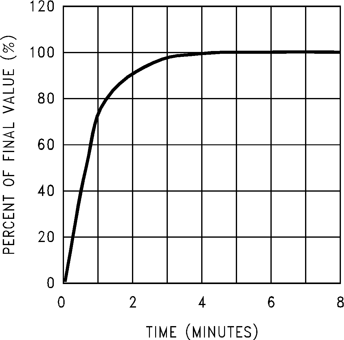
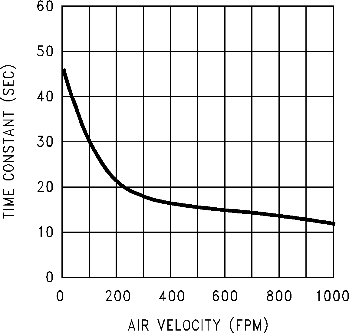 Figure 2. Thermal Time Constant
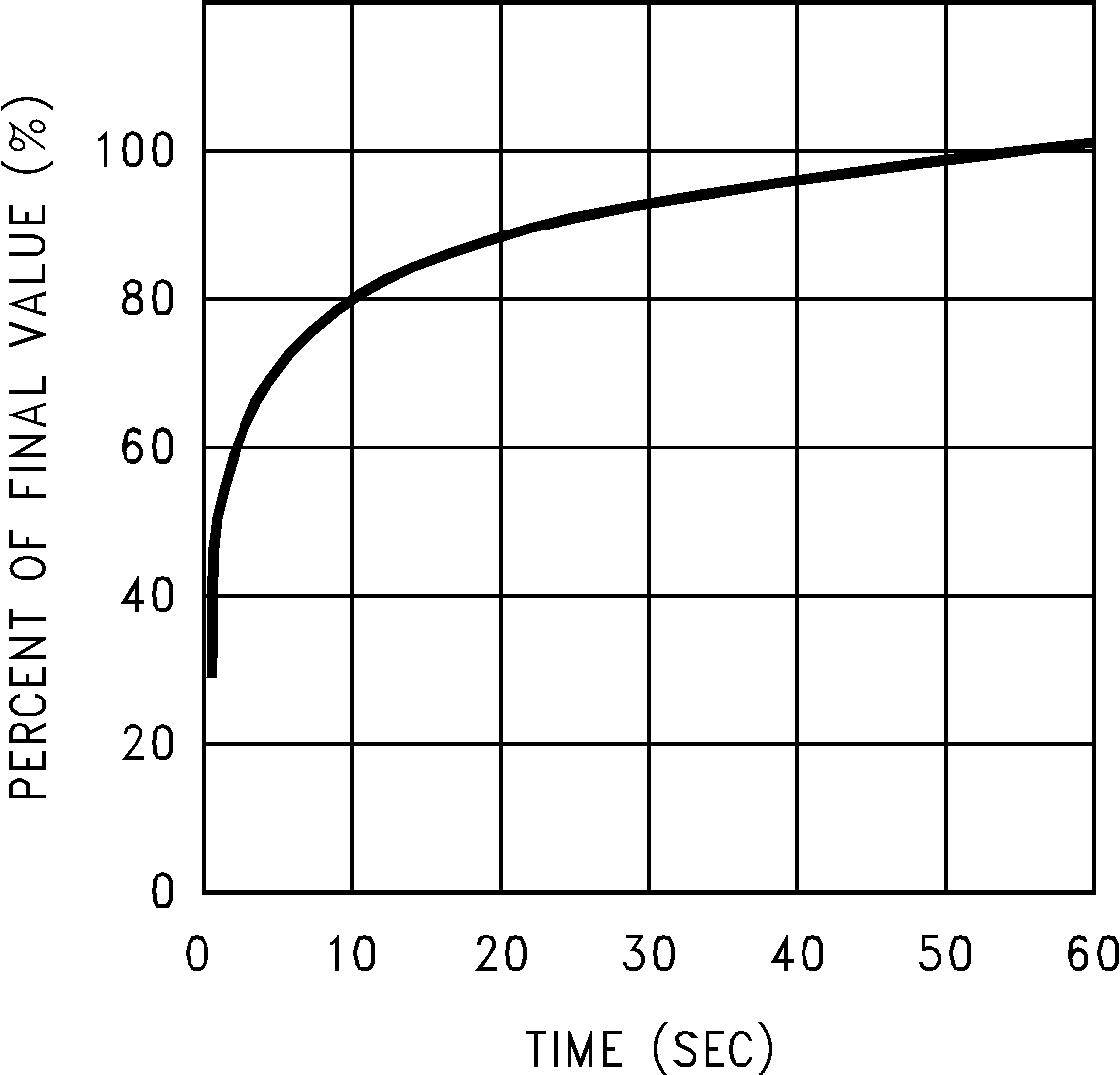
With Heat Sink
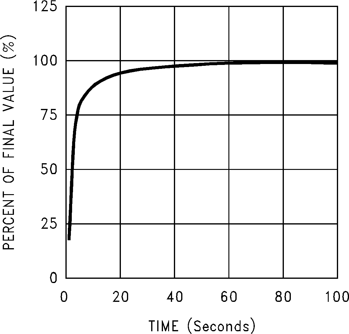 Figure 6. Thermal Response in Still Air Without a Heat Sink
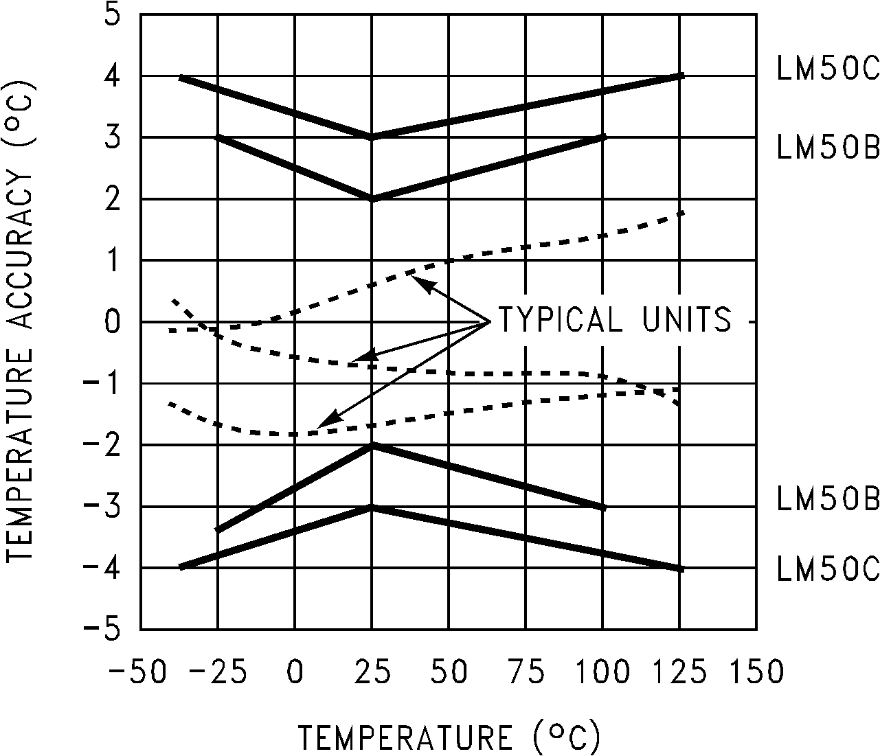
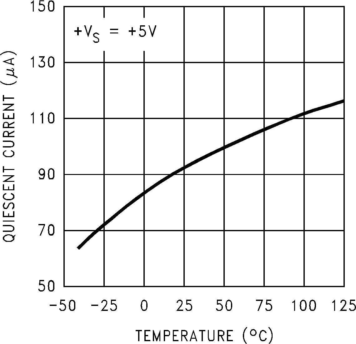
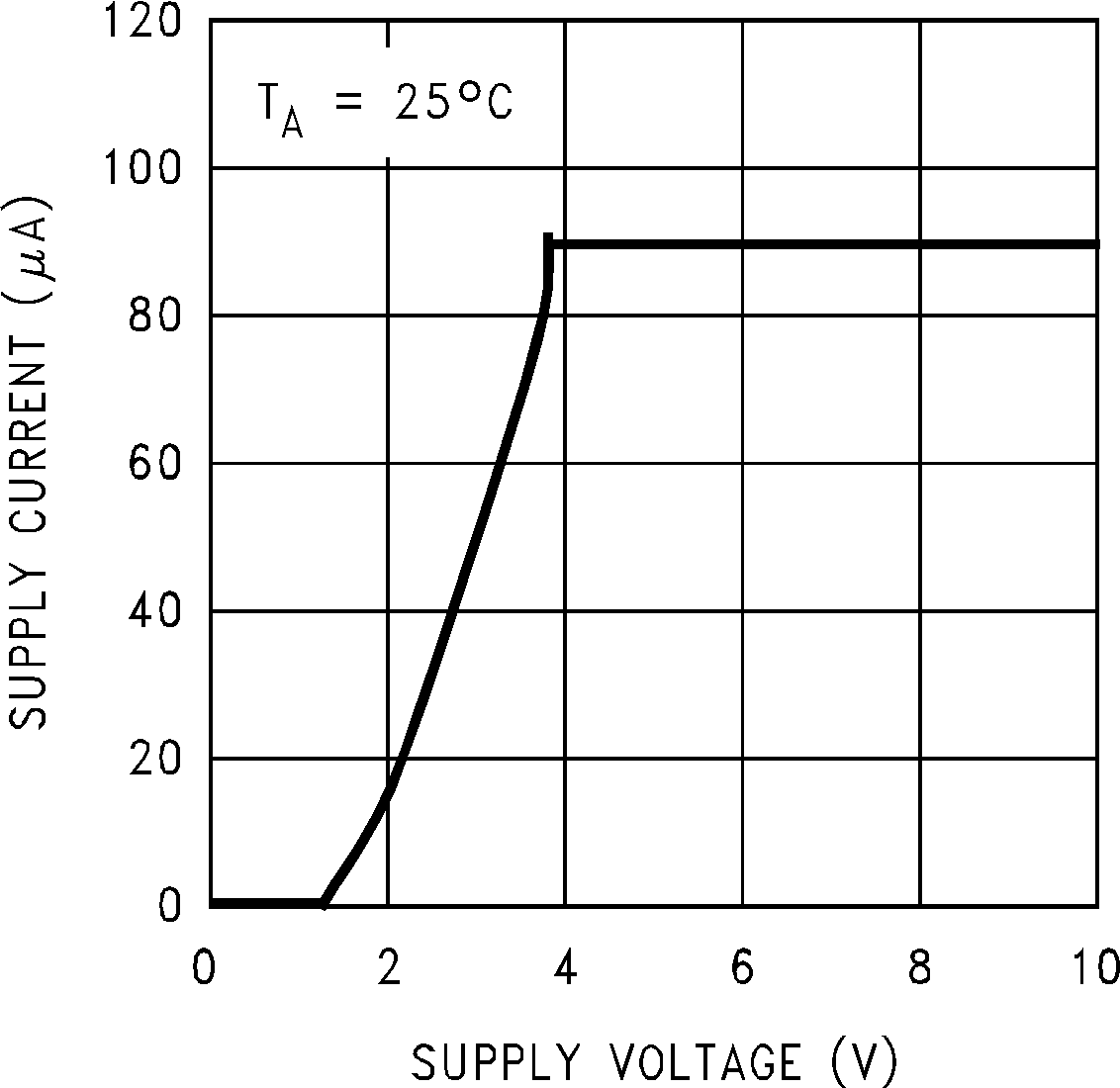 Figure 10. Supply Voltage vs Supply Current
