SNVS397E September 2005 – November 2016 LM5005
PRODUCTION DATA.
- 1 Features
- 2 Applications
- 3 Description
- 4 Revision History
- 5 Pin Configuration and Functions
- 6 Specifications
- 7 Detailed Description
-
8 Application and Implementation
- 8.1 Application Information
- 8.2
Typical Application
- 8.2.1 Design Requirements
- 8.2.2
Detailed Design Procedure
- 8.2.2.1 Frequency Set Resistor (RT)
- 8.2.2.2 Inductor (LF)
- 8.2.2.3 Ramp Capacitor (CRAMP)
- 8.2.2.4 Output Capacitors (COUT)
- 8.2.2.5 Schottky Diode (DF)
- 8.2.2.6 Input Capacitors (CIN)
- 8.2.2.7 VCC Capacitor (CVCC)
- 8.2.2.8 Bootstrap Capacitor (CBST)
- 8.2.2.9 Soft Start Capacitor (CSS)
- 8.2.2.10 Feedback Resistors (RFB1 and RFB2)
- 8.2.2.11 RC Snubber (RS and CS)
- 8.2.2.12 Compensation Components (RC1, CC1, CC2)
- 8.2.2.13 Bill of Materials
- 8.2.3 Application Curves
- 9 Power Supply Recommendations
- 10Layout
- 11Device and Documentation Support
- 12Mechanical, Packaging, and Orderable Information
Package Options
Mechanical Data (Package|Pins)
- PWP|20
Thermal pad, mechanical data (Package|Pins)
- PWP|20
Orderable Information
10 Layout
10.1 Layout Guidelines
PC board layout is an important and critical part of any DC-DC converter design. The performance of any switching converter depends as much upon the layout of the PCB as the component selection. Poor layout disrupts the performance of a switching converter and surrounding circuitry by contributing to EMI, ground bounce, conduction loss in the traces, and thermal problems. Erroneous signals can reach the DC-DC converter, possibly resulting in poor regulation or instability. There are several paths that conduct high slew-rate currents or voltages that can interact with stray inductance or parasitic capacitance to generate noise and EMI or degrade the power-supply performance.
The following guidelines serve to help users to design a PCB with the best power conversion performance, thermal performance, and minimized generation of unwanted EMI.
- In a buck regulator there are two critical current conduction loops. The first loop starts from the input capacitors to the LM5005's VIN pins, to the SW pin, to the inductor and then out to the load. The second loop starts from the output capacitors' return terminals, to the LM5005's PGND pins, to the IS pins, to the freewheeling diode's anode, to the inductor and then out to the load. Minimizing the effective area of these two loops reduces the stray inductance and minimizes noise and possible erratic operation.
- Place the input capacitors close to the LM5005's VIN pins and exposed pad that is connected to PGND pins. Place the inductor as close as possible to the SW pins and output capacitors. As described further in PCB Layout for EMI Reduction, this placement serves to minimize the area of switching current loops and reduce the resistive loss of the high current path. Ideally, use a ground plane on the top layer that connects the PGND pins, the exposed pad of the device, and the return terminals of the input and output capacitors. For more details, see the board layout detailed in LM5005 EVM user's guide AN-1748 LM5005 Evaluation Board (SNVA298).
- Minimize the copper area of the switch node. Route the two SW pins on a single top-layer plane to the inductor terminal using a wide trace to minimize conduction loss. The inductor can be placed on the bottom side of the PCB relative to the LM5005, but take care to avoid any coupling of the inductor's magnetic field to sensitive feedback or compensation traces.
- Use a solid ground plane on layer two of the PCB, particularly underneath the LM5005 and power stage components. This plane functions as a noise shield and also as a heat dissipation path.
- Make input and output power bus connections as wide and short as possible to reduce voltage drops on the input and output of the converter and to improve efficiency. Use copper planes on top to connect the multiple VIN pins and PGND pins together.
- Provide enough PCB area for proper heat-sinking. As stated in Thermal Design, use enough copper area to ensure a low RθJA commensurate with the maximum load current and ambient temperature. Make the top and bottom PCB layers with two ounce copper thickness and no less than one ounce. Use an array of heat-sinking vias to connect the exposed pad to the ground plane on the bottom PCB layer. If the PCB has multiple copper layers as recommended, connect these thermal vias to the inner layer heat-spreading ground planes.
- Route the sense trace from the VOUT point of regulation to the feedback resistors away from the SW pins and inductor to avoid contaminating this feedback signal with switching noise. This routing is most important when high resistances are used to set the output voltage. Routing the feedback trace on a different layer than the inductor and SW node trace is recommended such that a ground plane exists between the sense trace and inductor or SW node polygon to provide further cancellation of EMI on the feedback trace.
- If voltage accuracy at the load is important, ensure that the feedback voltage sense is made directly at the load terminals. Doing so corrects for voltage drops in the PCB planes and traces and provides optimal output voltage set-point accuracy and load regulation. Place the feedback resistor divider closer to the FB pin, rather than close to the load, because the FB node is the input to the error amplifier and is thus noise sensitive.
- COMP is a also noise-sensitive node. Place the compensation components as close as possible to the FB and COMP pins.
- Place the components for RT, CSS, CRAMP and CVCC close to their respective pins. Connect all of the signal components' ground return connections directly to the LM5005's AGND pin. Connect the AGND and PGND pins together at the LM5005's exposed pad using the topside copper area covering the entire underside of the device. Connect several vias within this underside copper area to the PCB's internal ground plane.
- See Related Documentation for additional important guidelines.
10.1.1 PCB Layout for EMI Reduction
Radiated EMI generated by high slew-rate current edges relates to pulsating currents in switching converters. The larger area covered by the path of a pulsing current, the more electromagnetic emission is generated. The key to reducing radiated EMI is to identify the pulsing current path and minimize the area of that path.
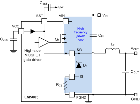
The important high-frequency switching power loop (or hot loop) of the LM5005 power stage is denoted in blue in Figure 34. The topological architecture of a buck converter means that particularly high di/dt current exists in this loop as current commutates between the externally-connected Schottky diode and the integrated high-side MOSFET during switching transitions. As such, it becomes mandatory to minimize this effective loop area, with an eye to reducing the layout-induced parasitic or stray inductances that cause excessive SW voltage overshoot and ringing, noise and ground bounce.
In general, MOSFET switching behavior and the consequences for waveform ringing, power dissipation, device stress and EMI are correlated with the parasitic inductances of the power loop. It follows that the cumulative benefits of reducing the switching loop area are increased reliability and robustness owing to lower power MOSFET voltage and current stress, increased margin for input voltage transients, and easier EMI filtering (particularly in the more challenging high-frequency band above 30 MHz).
 Figure 34. LM5005 Power Stage Circuit Switching Loops
High-frequency ceramic bypass capacitors at the input side provide the primary path for the high di/dt components of the pulsing current. Position low-ESL ceramic bypass capacitors with low-inductance, short trace routes to the VIN and PGND pins. Keep the SW trace connecting to the inductor as short as possible, and just wide enough to carry the load current without excessive heating. Use short, thick traces or copper polygon pours (shapes) for current conduction paths to minimize parasitic resistance. Place the output capacitors close to the VOUT side of the inductor and route the return connection using GND plane copper back to the PGND pins and the exposed pad of the LM5005.
10.1.2 Thermal Design
As with any power conversion device, the LM5005 dissipates internal power while operating. The effect of this power dissipation is to raise the internal junction temperature of the LM5005 above ambient. The junction temperature (TJ) is a function of the ambient temperature (TA), the power dissipation (PD) and the effective thermal resistance of the device and PCB combination (RθJA). The maximum operating junction temperature for the LM5005 is 125°C, thus establishing a limit on the maximum device power dissipation and therefore the load current at high ambient temperatures. Equation 21 and Equation 22 show the relationships between these parameters.


An approximation for the inductor power loss in Equation 21 includes a factor of 1.5 for the core losses. Also, if a snubber is used, estimate its power loss by observation of the resistor voltage drop at both turnon and turnoff switching transitions.
High ambient temperatures and large values of RθJA reduce the maximum available output current. If the junction temperature exceeds 165°C, the LM5005 cycles in and out of thermal shutdown. Thermal shutdown may be a sign of inadequate heat-sinking or excessive power dissipation. Improve PCB heat-sinking by using more thermal vias, a larger board, or more heat-spreading layers within that board.
As stated in Semiconductor and IC Package Thermal Metrics (SPRA953), the values given in Thermal Information are not always valid for design purposes to estimate the thermal performance of the application. The values reported in this table are measured under a specific set of conditions that are seldom obtained in an actual application. The effective RθJA is a critical parameter and depends on many factors (such as power dissipation, air temperature, PCB area, copper heat-sink area, number of thermal vias under the package, air flow, and adjacent component placement). The LM5005's exposed pad has a direct thermal connection to PGND. This pad must be soldered directly to the PCB copper ground plane to provide an effective heat-sink and proper electrical connection. Use the documents listed in Documentation Support as a guide for optimized thermal PCB design and estimating RθJA for a given application environment.
10.1.3 Ground Plane Design
As mentioned previously, using one of the inner PCB layers as a solid ground plane is recommended. A ground plane offers shielding for sensitive circuits and traces and also provides a quiet reference potential for the control circuitry. Connect the PGND pins to the system ground plane using an array of vias under the LM5005's exposed pad. Also connect the PGND pins directly to the return terminals of the input and output capacitors. The PGND net contains noise at the switching frequency and can bounce because of load current variations. The power traces for PGND, VIN, and SW can be restricted to one side of the ground plane. The other side of the ground plane contains much less noise and is ideal for sensitive analog trace routes.
10.2 Layout Example
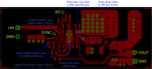
 Figure 35. Component Side
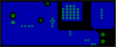
 Figure 36. Solder Side (Viewed From Top)
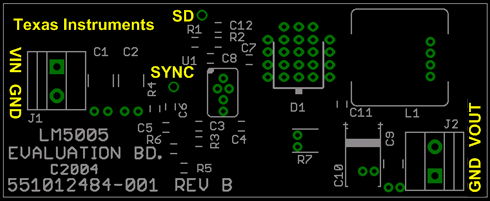
 Figure 37. Silkscreen