SNVS280I April   2004  – October 2018 LM5008

PRODUCTION DATA.  

  1. Features
  2. Applications
  3. Description
    1.     Device Images
      1.      Typical Application Circuit and Block Diagram
  4. Revision History
  5. Pin Configuration and Functions
    1.     Pin Functions
  6. Specifications
    1. 6.1 Absolute Maximum Ratings
    2. 6.2 ESD Ratings
    3. 6.3 Recommended Operating Conditions
    4. 6.4 Thermal Information
    5. 6.5 Electrical Characteristics
    6. 6.6 Switching Characteristics
    7. 6.7 Typical Characteristics
  7. Detailed Description
    1. 7.1 Overview
    2. 7.2 Functional Block Diagram
    3. 7.3 Feature Description
      1. 7.3.1 Hysteretic Control Circuit Overview
      2. 7.3.2 High Voltage Start-Up Regulator
      3. 7.3.3 Regulation Comparator
      4. 7.3.4 Overvoltage Comparator
      5. 7.3.5 On-Time Generator and Shutdown
      6. 7.3.6 Current Limit
      7. 7.3.7 N-Channel Buck Switch and Driver
      8. 7.3.8 Thermal Protection
    4. 7.4 Device Functional Modes
      1. 7.4.1 Shutdown Mode
      2. 7.4.2 Active Mode
  8. Application and Implementation
    1. 8.1 Application Information
      1. 8.1.1 Minimum Load Current
    2. 8.2 Typical Application
      1. 8.2.1 Design Requirements
      2. 8.2.2 Detailed Design Procedure
        1. 8.2.2.1 Custom Design With WEBENCH® Tools
      3. 8.2.3 Application Curves
  9. Power Supply Recommendations
  10. 10Layout
    1. 10.1 Layout Guidelines
    2. 10.2 Layout Examples
  11. 11Device and Documentation Support
    1. 11.1 Device Support
      1. 11.1.1 Third-Party Products Disclaimer
      2. 11.1.2 Custom Design With WEBENCH® Tools
      3. 11.1.3 Development Support
    2. 11.2 Documentation Support
      1. 11.2.1 Related Documentation
        1. 11.2.1.1 PCB Layout Resources
        2. 11.2.1.2 Thermal Design Resources
    3. 11.3 Receiving Notification of Documentation Updates
    4. 11.4 Community Resources
    5. 11.5 Trademarks
    6. 11.6 Electrostatic Discharge Caution
    7. 11.7 Glossary
  12. 12Mechanical, Packaging, and Orderable Information

Package Options

Mechanical Data (Package|Pins)
Thermal pad, mechanical data (Package|Pins)
Orderable Information

High Voltage Start-Up Regulator

The LM5008 contains an internal high voltage start-up regulator. The input pin (VIN) can be connected directly to the line voltages up to 95 Volts, with transient capability to 100 V. The regulator is internally current limited to 9.5 mA at VCC. Upon power up, the regulator sources current into the external capacitor at VCC (C3). When the voltage on the VCC pin reaches the undervoltage lockout threshold of 6.3 V, the buck switch is enabled.

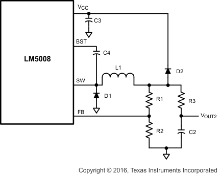
In applications involving a high value for VIN, where power dissipation in the VCC regulator is a concern, an auxiliary voltage can be diode connected to the VCC pin. Setting the auxiliary voltage to 8 V to 14 V shuts off the internal regulator, reducing internal power dissipation. See Figure 8. The current required into the VCC pin is shown in Figure 1.
LM5008 20097906.gifFigure 8. Self-Biased Configuration