SNVS583H
March 2009 – October 2018
LM5008A
PRODUCTION DATA.
1
Features
2
Applications
3
Description
Device Images
Typical Application, Basic Step-Down Regulator
4
Revision History
5
Pin Configuration and Functions
Pin Functions
6
Specifications
6.1
Absolute Maximum Ratings
6.2
ESD Ratings
6.3
Recommended Operating Conditions
6.4
Thermal Information
6.5
Electrical Characteristics
6.6
Switching Characteristics
6.7
Typical Characteristics
7
Detailed Description
7.1
Overview
7.2
Functional Block Diagram
7.3
Feature Description
7.3.1
Control Circuit Overview
7.3.2
Start-Up Regulator (VCC)
7.3.3
Regulation Comparator
7.3.4
Overvoltage Comparator
7.3.5
On-Time Generator and Shutdown
7.3.6
Current Limit
7.3.7
N-Channel Buck Switch and Driver
7.3.8
Thermal Protection
7.4
Device Functional Modes
7.4.1
Shutdown Mode
7.4.2
Active Mode
8
Application and Implementation
8.1
Application Information
8.2
Typical Application
8.2.1
Design Requirements
8.2.2
Detailed Design Procedure
8.2.2.1
Custom Design With WEBENCH® Tools
8.2.2.2
Selection Of External Components
8.2.2.3
Low-Output Ripple Configurations
8.2.3
Application Curves
9
Power Supply Recommendations
10
Layout
10.1
Layout Guidelines
10.2
Layout Example
11
Device and Documentation Support
11.1
Device Support
11.1.1
Third-Party Products Disclaimer
11.1.2
Custom Design With WEBENCH® Tools
11.1.3
Development Support
11.2
Documentation Support
11.2.1
Related Documentation
11.2.1.1
PCB Layout Resources
11.2.1.2
Thermal Design Resources
11.3
Receiving Notification of Documentation Updates
11.4
Community Resources
11.5
Trademarks
11.6
Electrostatic Discharge Caution
11.7
Glossary
12
Mechanical, Packaging, and Orderable Information
Package Options
Mechanical Data (Package|Pins)
NGU|8
MPDS407A
DGK|8
MPDS028E
Thermal pad, mechanical data (Package|Pins)
Orderable Information
snvs583h_oa
snvs583h_pm
6.7
Typical Characteristics
Figure 1.
Efficiency vs Load Current and V
IN
(Circuit of
Figure 10
)
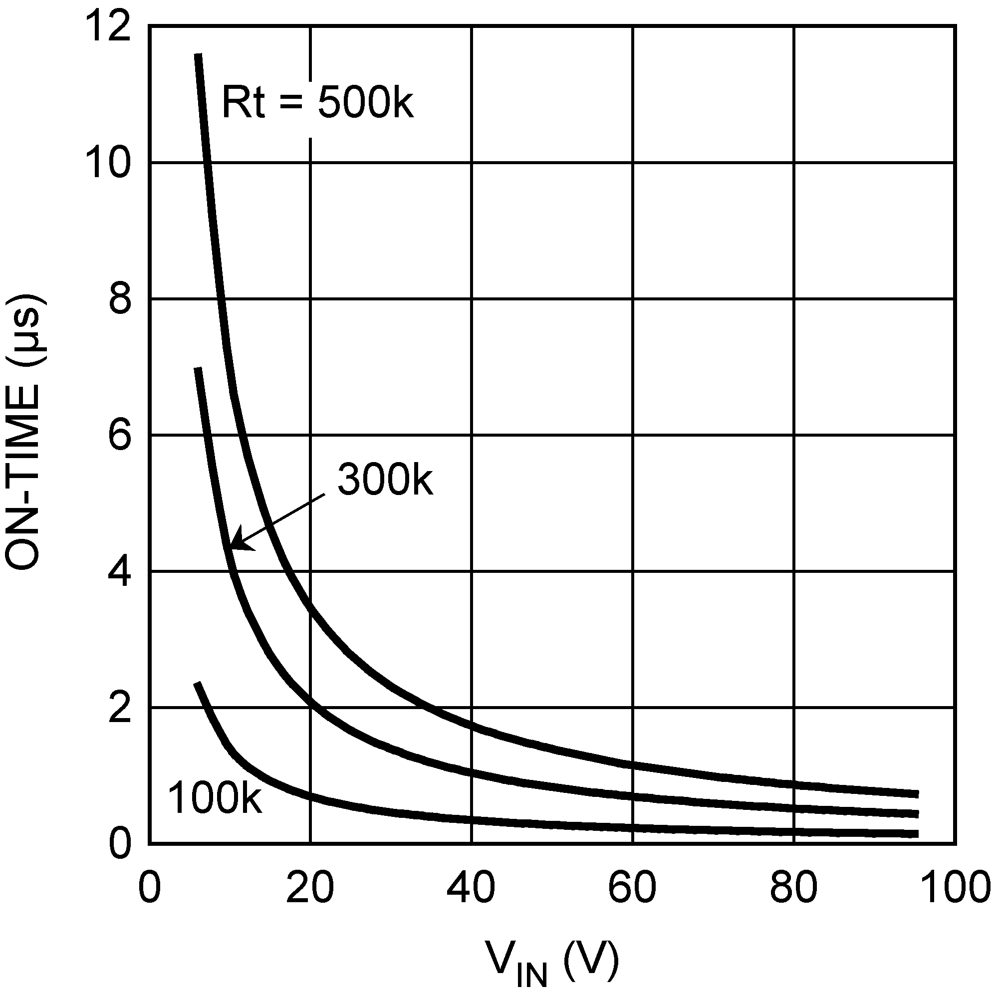
Figure 3.
On-Time vs Input Voltage and R
T
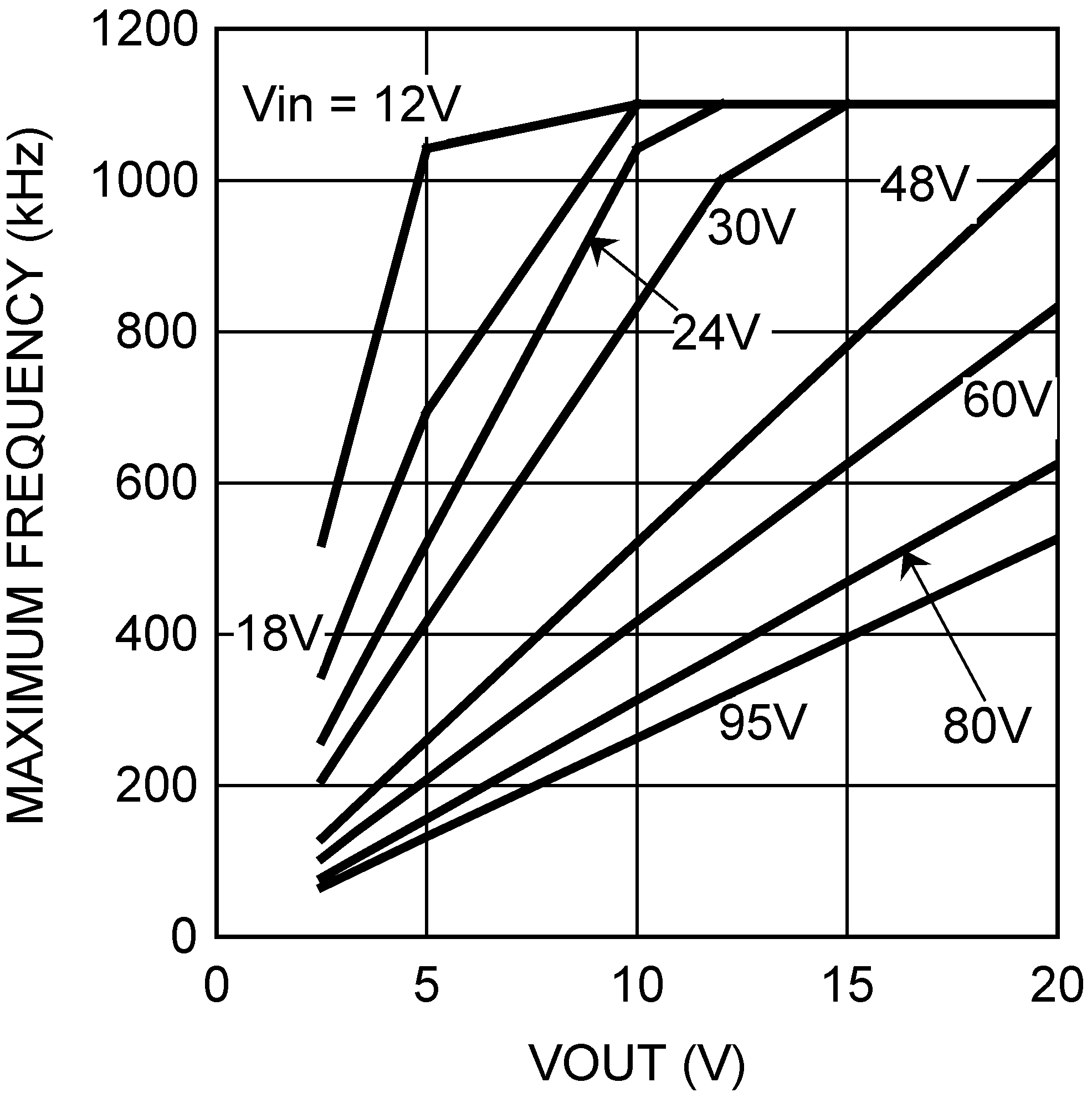
Figure 5.
Maximum Frequency vs V
OUT
and V
IN
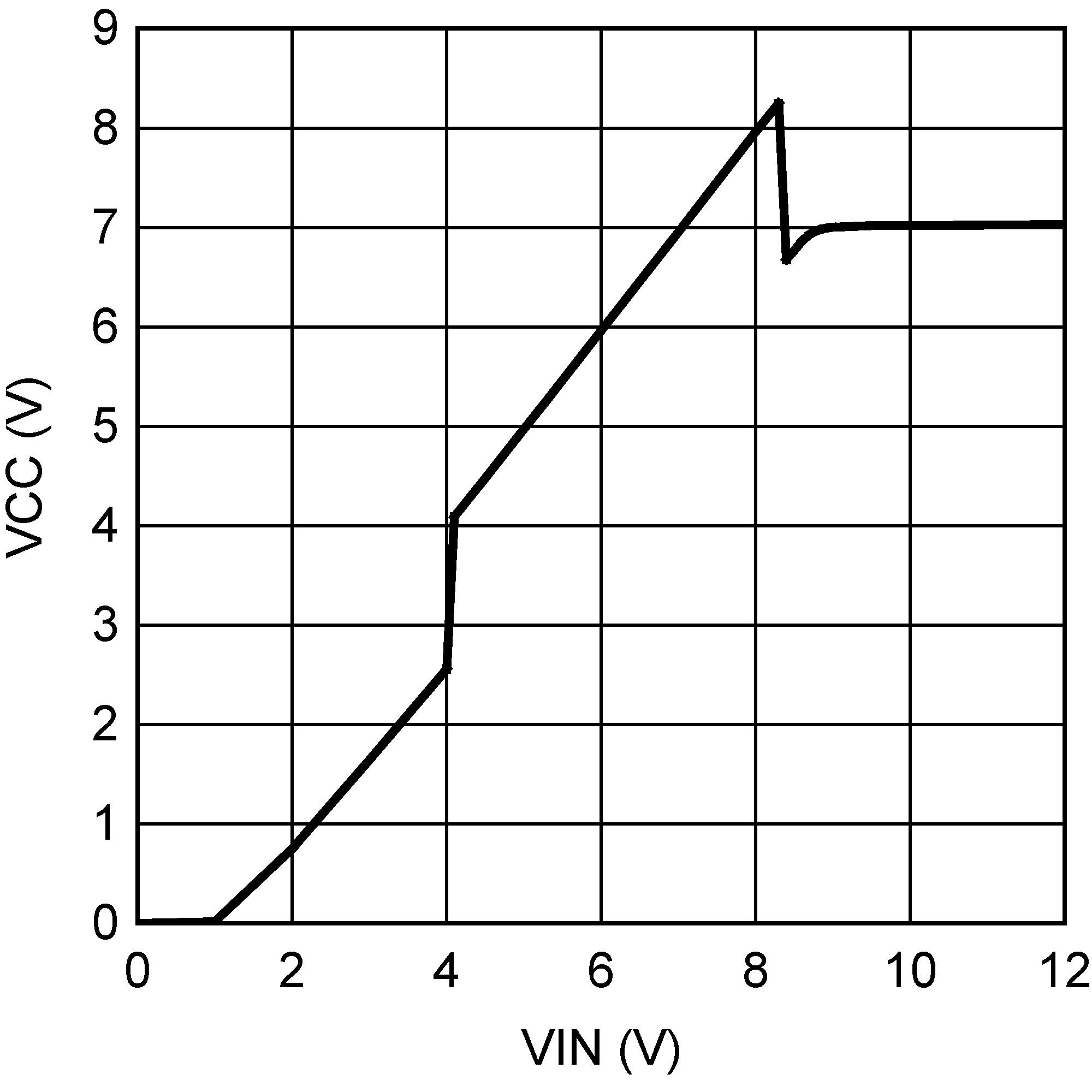
Figure 2.
V
CC
vs V
IN
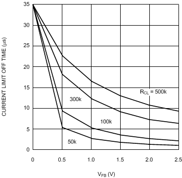
Figure 4.
Current Limit Off-Time vs V
FB
and R
CL
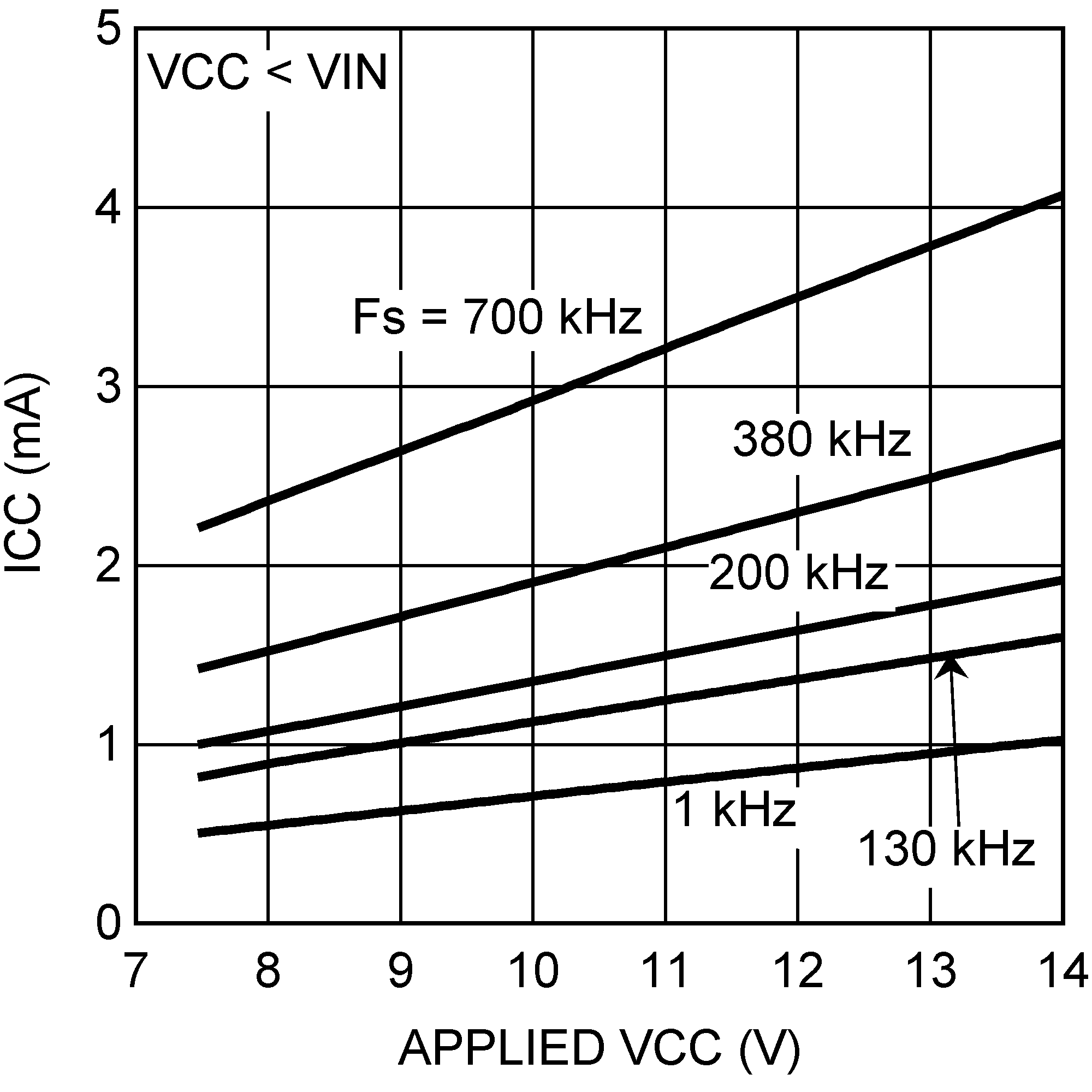
Figure 6.
I
CC
Current vs Applied V
CC
Voltage