SNVS402I February 2006 – May 2021 LM5009
PRODUCTION DATA
- 1 Features
- 2 Applications
- 3 Description
- 4 Revision History
- 5 Pin Configuration and Functions
- 6 Specifications
- 7 Detailed Description
-
8 Application and Implementation
- 8.1 Application Information
- 8.2
Typical Application
- 8.2.1 Design Requirements
- 8.2.2
Detailed Design Procedure
- 8.2.2.1 Output Resistor Divider Selection
- 8.2.2.2 Frequency Selection
- 8.2.2.3 Inductor Selection
- 8.2.2.4 VCC and Bootstrap Capacitor
- 8.2.2.5 Output Capacitor Selection
- 8.2.2.6 Current Limit Off-Timer Setting
- 8.2.2.7 Rectifier Diode Selection
- 8.2.2.8 Input Capacitor Selection
- 8.2.2.9 Ripple Configuration
- 8.2.3 Application Curves
- 8.3 Do's and Don'ts
- 9 Power Supply Recommendations
- 10Layout
- 11Device and Documentation Support
- 12Mechanical, Packaging, and Orderable Information
Package Options
Mechanical Data (Package|Pins)
Thermal pad, mechanical data (Package|Pins)
Orderable Information
5 Pin Configuration and Functions
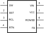
 Figure 5-1 DGK, NGU Packages8-Pin VSSOP, WSONTop View
Table 5-1 Pin Functions
| PIN | I/O | DESCRIPTION | |
|---|---|---|---|
| NAME | NO. | ||
| BST | 2 | I | Boost pin. An external capacitor is required between the BST and SW pins. A 0.022-µF ceramic capacitor is recommended. An internal diode charges the capacitor from VCC. |
| EP | — | — | Exposed pad (WSON package only). Exposed metal pad on the underside of the device. Connecting this pad to the PC board ground plane is recommended to aid in heat dissipation. |
| FB | 5 | I | Feedback input from regulated output. This pin is connected to the inverting input of the internal regulation comparator. The regulation threshold is 2.5 V. |
| RCL | 3 | I | Current limit off-time set pin. A resistor between this pin and RTN sets the off-time when current limit is detected. The off-time is preset to 35 µs if FB = 0 V. |
| RON/SD | 6 | I | On-time set pin. A resistor between this pin and VIN sets the switch on-time as a function of VIN. The minimum recommended on-time is 250 ns at the maximum input voltage. This pin can be used for remote shutdown. |
| RTN | 4 | — | Ground pin. Ground for the entire circuit. |
| SW | 1 | O | Switching output. Power switching output. Connect to the inductor, recirculating diode, and bootstrap capacitor. |
| VCC | 7 | O | Output from the internal high-voltage startup regulator. Regulated at 7.0 V. If an auxiliary voltage is available to raise the voltage on this pin above the regulation set point (7 V), the internal series pass regulator shuts down, reducing the device power dissipation. Do not exceed 14 V. This voltage provides gate drive power for the internal buck switch. An internal diode is provided between this pin and the BST pin. A local 0.1-µF decoupling capacitor is required. |
| VIN | 8 | I | Input voltage. Recommended operating range: 9.5 V to 95 V. |