SNVS608H June 2009 – September 2016 LM5009A
PRODUCTION DATA.
- 1 Features
- 2 Applications
- 3 Description
- 4 Revision History
- 5 Pin Configuration and Functions
- 6 Specifications
- 7 Detailed Description
- 8 Application and Implementation
- 9 Power Supply Recommendations
- 10Layout
- 11Device and Documentation Support
- 12Mechanical, Packaging, and Orderable Information
Package Options
Mechanical Data (Package|Pins)
Thermal pad, mechanical data (Package|Pins)
Orderable Information
8 Application and Implementation
NOTE
Information in the following applications sections is not part of the TI component specification, and TI does not warrant its accuracy or completeness. TI’s customers are responsible for determining suitability of components for their purposes. Customers should validate and test their design implementation to confirm system functionality.
8.1 Application Information
The LM5009A is a nonsynchronous buck regulator designed to operate over a wide input voltage range and output current. Spreadsheet-based quick-start calculation tools and the on-line WEBENCH® software can be used to create a buck design along with the bill of materials, estimated efficiency, and the complete solution cost.
8.2 Typical Application
The final circuit is shown in Figure 10. The circuit was tested, and the resulting performance is shown in Figure 11 and Figure 12.
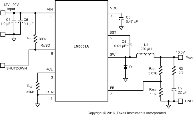 Figure 10. LM5009A Example Circuit
8.2.1 Design Requirements
A guide for determining the component values is illustrated with a design example. See Functional Block Diagram and the Bill of Materials listed in Table 2.
Table 1. Design Parameters
| PARAMETER | VALUE |
|---|---|
| Input voltage range | 12 V to 90 V |
| Output voltage | 10 V |
| Load current range | 100 mA to 150 mA |
8.2.2 Detailed Design Procedure
Table 2. Bill of Materials
| ITEM | DESCRIPTION | PART NUMBER | VALUE |
|---|---|---|---|
| C1 | Ceramic capacitor | TDK C4532X7R2A105M | 1 µF, 100 V |
| C2 | Ceramic capacitor | TDK C4532X7R1E226M | 22 µF, 25 V |
| C3 | Ceramic capacitor | Kemet C1206C474K5RAC | 0.47 µF, 50 V |
| C4 | Ceramic capacitor | Kemet C1206C103K5RAC | 0.01 µF, 50 V |
| C5 | Ceramic capacitor | TDK C3216X7R2A104M | 0.1 µF, 100 V |
| D1 | Schottky power diode | Diodes Inc. DFLS1100 | 100 V, 1 A |
| L1 | Power inductor | COILTRONICS DR125-221-R or TDK SLF10145T-221MR65 |
220 µH |
| RFB2 | Resistor | Vishay CRCW12063011F | 3.01 kΩ |
| RFB1 | Resistor | Vishay CRCW12061001F | 1 kΩ |
| R3 | Resistor | Vishay CRCW12063R30F | 3.3 Ω |
| RT | Resistor | Vishay CRCW12063093F | 309 kΩ |
| RCL | Resistor | Vishay CRCW12063163F | 316 kΩ |
| U1 | Switching regulator | Texas Instruments LM5009A | — |
8.2.2.1 RFB1 and RFB2
Because VFB = 2.5 V, the ratio of RFB2 to RFB1 calculates as 3:1. Standard values of 3.01 kΩ and 1 kΩ are chosen. Other values could be used as long as the 3:1 ratio is maintained.
8.2.2.2 Fs and RT
The recommended operating frequency range for the LM5009A is 50 kHz to 1.1 MHz. Unless the application requires a specific frequency, the choice of frequency is generally a compromise, because it affects the size of L1 and C2, and the switching losses. The maximum allowed frequency, based on a minimum ON time of 400 ns, is calculated with Equation 7.
For this exercise, FMAX = 277 kHz. From Equation 2, RT calculates to 260 kΩ. A standard value, 309-kΩ resistor is used to allow for tolerances in Equation 2, resulting in a frequency of 234 kHz.
8.2.2.3 L1
The main parameter affected by the inductor is the output current ripple amplitude. The choice of inductor value therefore depends on both the minimum and maximum load currents, keeping in mind that the maximum ripple current occurs at maximum VIN.
8.2.2.3.1 Minimum Load Current
To maintain continuous conduction at minimum IO (100 mA), the ripple amplitude (IOR) must be less than 200 mA peak-to-peak so the lower peak of the waveform does not reach zero. L1 is calculated using Equation 8.

At VIN = 90 V, L1(min) calculates to 190 µH. The next larger standard value (220 µH) is chosen and with this value IOR calculates to 173 mA peak-to-peak at VIN = 90 V, and 32 mA peak-to-peak at VIN = 12 V.
8.2.2.3.2 Maximum Load Current
At a load current of 150 mA, the peak of the ripple waveform must not reach the minimum value of the LM5009A’s current limit threshold (240 mA). Therefore, the ripple amplitude must be less than 180 mA peak-to-peak, which is already satisfied in the above calculation. With L1 = 220 µH, at maximum VIN and IO, the peak of the ripple is 236 mA. While L1 must carry this peak current without saturating or exceeding the temperature rating, it also must be capable of carrying the maximum value of the LM5009A’s current limit threshold (360 mA) without saturating, because the current limit is reached during startup.
The DC resistance of the inductor must be as low as possible to minimize the power loss.
8.2.2.4 C3
The capacitor on the VCC output provides not only noise filtering and stability, but the primary purpose is to prevent false triggering of the VCC UVLO at the buck switch on and off transitions. C3 must be no smaller than 0.47 µF.
8.2.2.5 C2 and R3
When selecting the output filter capacitor C2, the items to consider are ripple voltage due to the ESR, ripple voltage due to the capacitance, and the nature of the load.
8.2.2.6 ESR and R3
A low ESR for C2 is generally desirable so as to minimize power losses and heating within the capacitor. However, the regulator requires a minimum amount of ripple voltage at the feedback input for proper loop operation. For the LM5009A, the minimum ripple required at pin 5 is 25 mV peak-to-peak, requiring a minimum ripple at VOUT of 100 mV. Because the minimum ripple current (at minimum VIN) is 32 mA peak-to-peak, the minimum ESR required at VOUT is 100 mV / 32 mA = 3.12 Ω. Because quality capacitors for SMPS applications have an ESR considerably less than this, R3 is inserted as shown in Functional Block Diagram. R3’s value, along with C2’s ESR, must result in at least 25 mV peak-to-peak ripple at pin 5. Generally, R3 is 0.5 Ω to 4 Ω.
8.2.2.7 C2
C2 must generally be no smaller than 3.3 µF. Typically, the value is 10 µF to 20 µF with the optimum value determined by the load. If the load current is fairly constant, a small value suffices for C2. If the load current includes significant transients, a larger value is necessary. For each application, experimentation is required to determine the optimum values for R3 and C2.
8.2.2.8 RCL
When current limit is detected, the minimum OFF-time set by this resistor must be greater than the maximum normal OFF time, which occurs at maximum input voltage. Using Equation 4, the minimum ON time is 476 ns, yielding an OFF time of 3.8 µs (at 234 kHz). Due to the 25% tolerance on the ON time, the OFF-time tolerance is also 25%, yielding a maximum OFF time of 4.75 µs. Allowing for the response time of the current limit detection circuit (350 ns) increases the maximum OFF time to 5.1 µs. This is increased an additional 25% to 6.4 µs to allow for the tolerances of Equation 5. Using Equation 5, RCL calculates to 310 kΩ at VFB = 2.5 V. A standard value 316-kΩ resistor is used.
8.2.2.9 D1
The important parameters are reverse recovery time and forward voltage. The reverse recovery time determines how long the reverse current surge lasts each time the buck switch is turned on. The forward voltage drop is significant in the event the output is short-circuited as it is only this diode’s voltage which forces the inductor current to reduce during the forced OFF time. For this reason, a higher voltage is better, although that affects efficiency. A good choice is a Schottky power diode, such as the DFLS1100. The reverse voltage rating of D1 must be at least as great as the maximum VIN, and the current rating must be greater than the maximum current limit threshold (360 mA).
8.2.2.10 C1
C1 supplies most of the switch current during the ON time, and limit the voltage ripple at VIN, on the assumption that the voltage source feeding VIN has an output impedance greater than zero. At maximum load current, when the buck switch turns on, the current into pin 8 suddenly increases to the lower peak of the output current waveform, ramp up to the peak value, then drop to zero at turnoff. The average input current during this ON time is the load current (150 mA). For a worst-case calculation, C1 must supply this average load current during the maximum ON time. To keep the input voltage ripple to less than 2 V (for this exercise), C1 is calculated with Equation 9.

Quality ceramic capacitors in this value have a low ESR, which adds only a few millivolts to the ripple. It is the capacitance which is dominant in this case. To allow for the capacitor’s tolerance, temperature effects, and voltage effects, a 1-µF, 100-V X7R capacitor is used.
8.2.2.11 C4
The recommended value for C4 is 0.01 µF, as this is appropriate in the majority of applications. A high-quality ceramic capacitor, with low ESR is recommended as C4 supplies the surge current to charge the buck switch gate at turnon. A low ESR also ensures a quick recharge during each OFF time. At minimum VIN, when the ON time is at maximum, it is possible during start-up that C4 does not fully re-charge during each 300 ns OFF time. The circuit is not able to complete the start-up, and achieve output regulation. This can occur when the frequency is intended to be low (for example, RT = 500 K). In this case, C4 must be increased so it can maintain sufficient voltage across the buck switch driver during each ON time.
8.2.2.12 C5
This capacitor helps avoid supply voltage transients and ringing due to long lead inductance at VIN. TI recommends placing a low-ESR, 0.1-µF ceramic chip capacitor close to the LM5009A.
8.2.2.13 Ripple Configuration
The LM5009A uses a constant-ON-time (COT) control scheme where the ON time is terminated by a one-shot and the OFF time is terminated by the feedback voltage (VFB) falling below the reference voltage. Therefore, for stable operation, the feedback voltage must decrease monotonically in phase with the inductor current during the OFF time. Furthermore, this change in feedback voltage (VFB) during OFF time must be large enough to dominate any noise present at the feedback node.
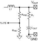
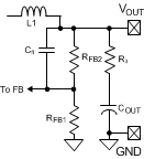
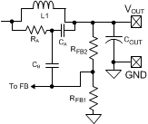
Table 3 presents three different methods for generating appropriate voltage ripple at the feedback node. Type 1 and type 2 ripple circuits couple the ripple from the output of the converter to the feedback node (FB). The output voltage ripple has two components:
- Capacitive ripple caused by the inductor current ripple charging or discharging the output capacitor.
- Resistive ripple caused by the inductor current ripple flowing through the ESR of the output capacitor and R3.
The capacitive ripple is out of phase with the inductor current. As a result, the capacitive ripple does not decrease monotonically during the OFF time. The resistive ripple is in phase with the inductor current and decreases monotonically during the OFF time. The resistive ripple must exceed the capacitive ripple at output (VOUT) for stable operation. If this condition is not satisfied, then unstable switching behavior is observed in COT converters with multiple ON-time bursts in close succession followed by a long OFF time.
The type 3 ripple method uses a ripple injection circuit with RA, CA, and the switch node (SW) voltage to generate a triangular ramp. This triangular ramp is then ac-coupled into the feedback node (FB) using the capacitor CB. This circuit is suited for applications where low output voltage ripple is imperative because this circuit does not use the output voltage ripple.
Table 3. Ripple Configuration
| TYPE 1 | TYPE 2 | TYPE 3 |
|---|---|---|
| Lowest cost | Reduced ripple | Minimum ripple |
 |
 |
 |
|
Equation 10.
 |
Equation 11.
 |
Equation 12.
 |
See AN-1481 Controlling Output Ripple and Achieving ESR Independence in Constant On-Time (COT) Regulator Designs (SNVA166) for more details on each ripple generation method.
8.2.3 Application Curves
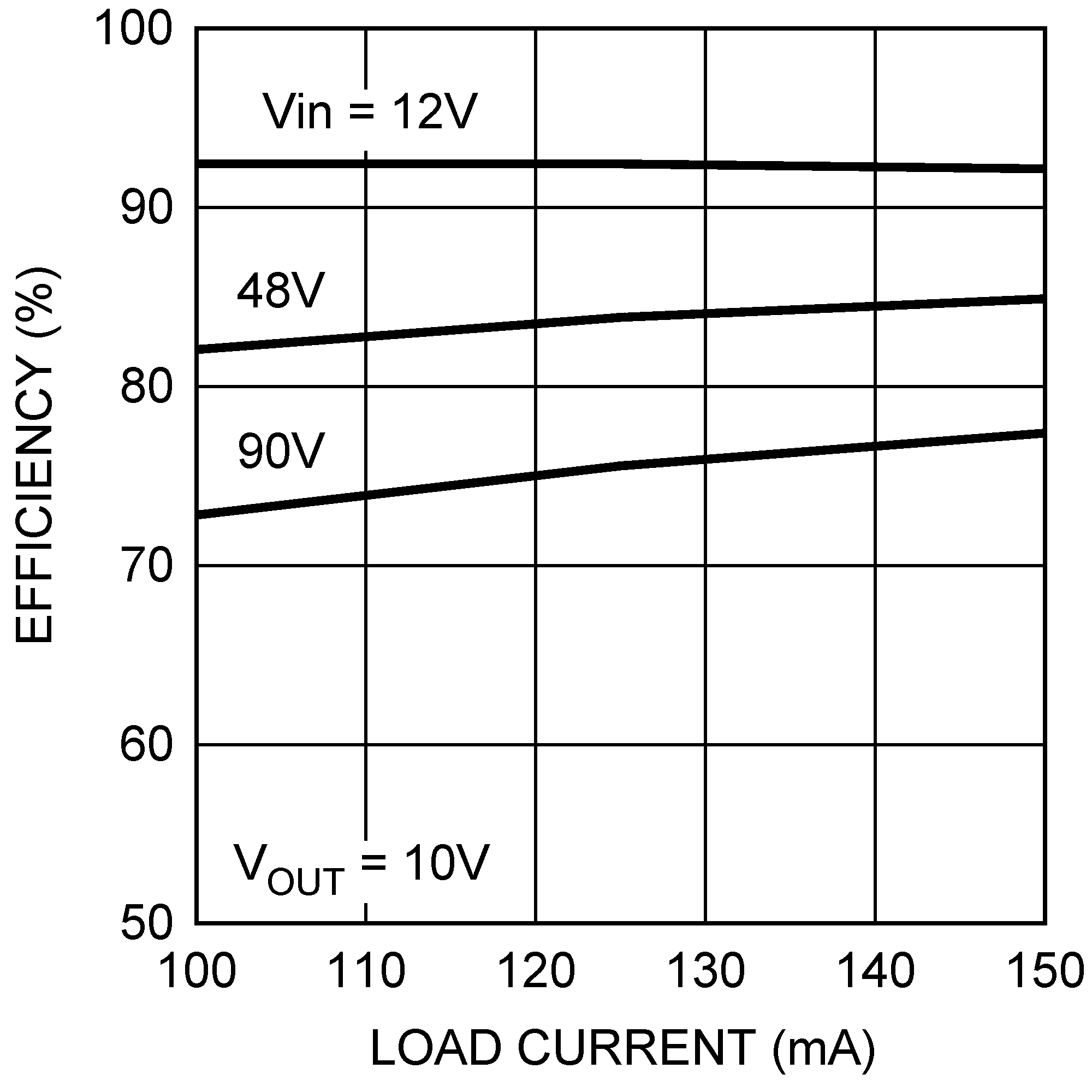 Figure 11. Efficiency vs Load Current and VIN
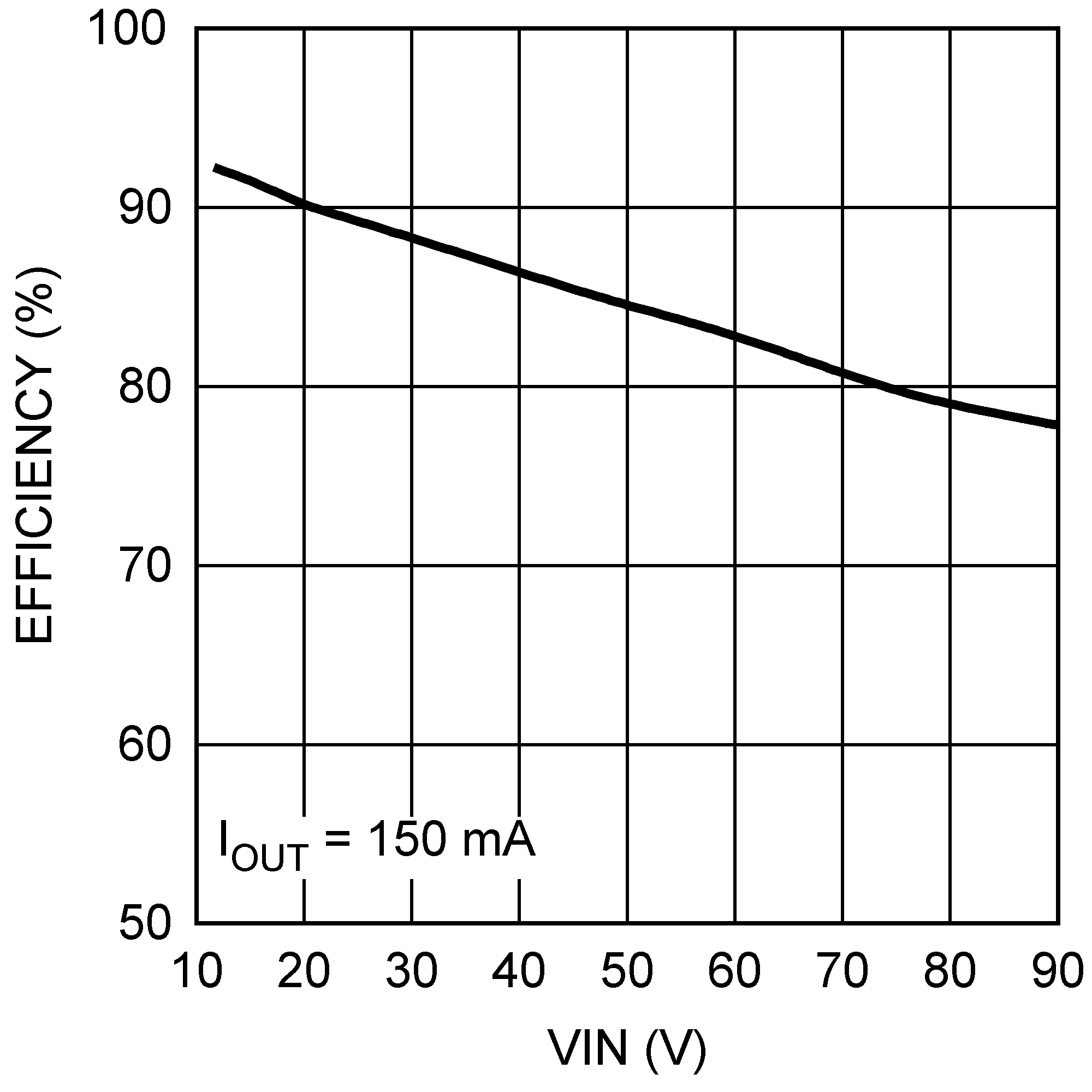 Figure 12. Efficiency vs VIN