SNVSC26 October   2022 LM5012-Q1

PRODUCTION DATA  

  1. Features
  2. Applications
  3. Description
  4. Revision History
  5. Device Comparison Table
  6. Pin Configuration and Functions
  7. Specifications
    1. 7.1 Absolute Maximum Ratings
    2. 7.2 ESD Ratings
    3. 7.3 Recommended Operating Conditions
    4. 7.4 Thermal Information
    5. 7.5 Electrical Characteristics
    6. 7.6 Typical Characteristics
  8. Detailed Description
    1. 8.1 Overview
    2. 8.2 Functional Block Diagram
    3. 8.3 Feature Description
      1. 8.3.1  Control Architecture
      2. 8.3.2  Internal VCC Regulator and Bootstrap Capacitor
      3. 8.3.3  Regulation Comparator
      4. 8.3.4  Internal Soft Start
      5. 8.3.5  On-Time Generator
      6. 8.3.6  Current Limit
      7. 8.3.7  N-Channel Buck Switch and Driver
      8. 8.3.8  Schottky Diode Selection
      9. 8.3.9  Enable/Undervoltage Lockout (EN/UVLO)
      10. 8.3.10 Power Good (PGOOD)
      11. 8.3.11 Thermal Protection
    4. 8.4 Device Functional Modes
      1. 8.4.1 Shutdown Mode
      2. 8.4.2 Standby Mode
      3. 8.4.3 Active Mode
      4. 8.4.4 Sleep Mode
  9. Application and Implementation
    1. 9.1 Application Information
    2. 9.2 Typical Application
      1. 9.2.1 Design Requirements
      2. 9.2.2 Detailed Design Procedure
        1. 9.2.2.1 Custom Design With WEBENCH® Tools
        2. 9.2.2.2 Switching Frequency (RRON)
        3. 9.2.2.3 Buck Inductor (LO)
        4. 9.2.2.4 Output Capacitor (COUT)
        5. 9.2.2.5 Input Capacitor (CIN)
        6. 9.2.2.6 Type 3 Ripple Network
      3. 9.2.3 Application Curves
    3. 9.3 Power Supply Recommendations
    4. 9.4 Layout
      1. 9.4.1 Layout Guidelines
        1. 9.4.1.1 Compact PCB Layout for EMI Reduction
        2. 9.4.1.2 Feedback Resistors
      2. 9.4.2 Layout Example
        1. 9.4.2.1 Thermal Considerations
  10. 10Device and Documentation Support
    1. 10.1 Device Support
      1. 10.1.1 Third-Party Products Disclaimer
      2. 10.1.2 Development Support
        1. 10.1.2.1 Custom Design With WEBENCH® Tools
    2. 10.2 Documentation Support
      1. 10.2.1 Related Documentation
    3. 10.3 Receiving Notification of Documentation Updates
    4. 10.4 Support Resources
    5. 10.5 Trademarks
    6. 10.6 Electrostatic Discharge Caution
    7. 10.7 Glossary
  11. 11Mechanical, Packaging, and Orderable Information

Package Options

Mechanical Data (Package|Pins)
Thermal pad, mechanical data (Package|Pins)
Orderable Information

Description

The LM5012-Q1 non-synchronous buck converter is designed to regulate over a wide input voltage range, minimizing the need for external surge suppression components. A minimum controllable on time of 50 ns facilitates large step-down conversion ratio, enabling the direct step-down for 48 -V nominal input to low-voltage rails for reduced systems complexity and solution cost. The LM5012-Q1 operates during input voltage dips as low as 6 V, at nearly 100 % duty cycle if needed, making it an excellent choice for high-performance 48-V battery automotive application and MHEV/EV systems.

With an integrated high-side power MOSFET, the LM5012-Q1 delivers up to 2.5 A of output current. A constant on-time (COT) control architecture provides nearly constant switching frequency with excellent load and line transient response. Additional features of the LM5012-Q1 include ultra-low IQ operation for high light-load efficiency, innovative peak overcurrent protection, integrated VCC bias supply and bootstrap diode, precision enable and input UVLO, and thermal shutdown protection with automatic recovery. An open-drain PGOOD indicator provides sequencing, fault reporting, and output voltage monitoring.

The LM5012-Q12.5 A is qualified to automotive AEC-Q100 grade 1 and is available in a 8-pin SO PowerPAD™ integrated circuit package. The device 1.27-mm pin pitch provides adequate spacing for high-voltage applications.

Package Information
Part Number Package(1) Body Size (NOM)
LM5012-Q1 DDA (SO PowerPAD, 8) 4.89 mm × 3.90 mm
For all available packages, see the orderable addendum at the end of the data sheet.
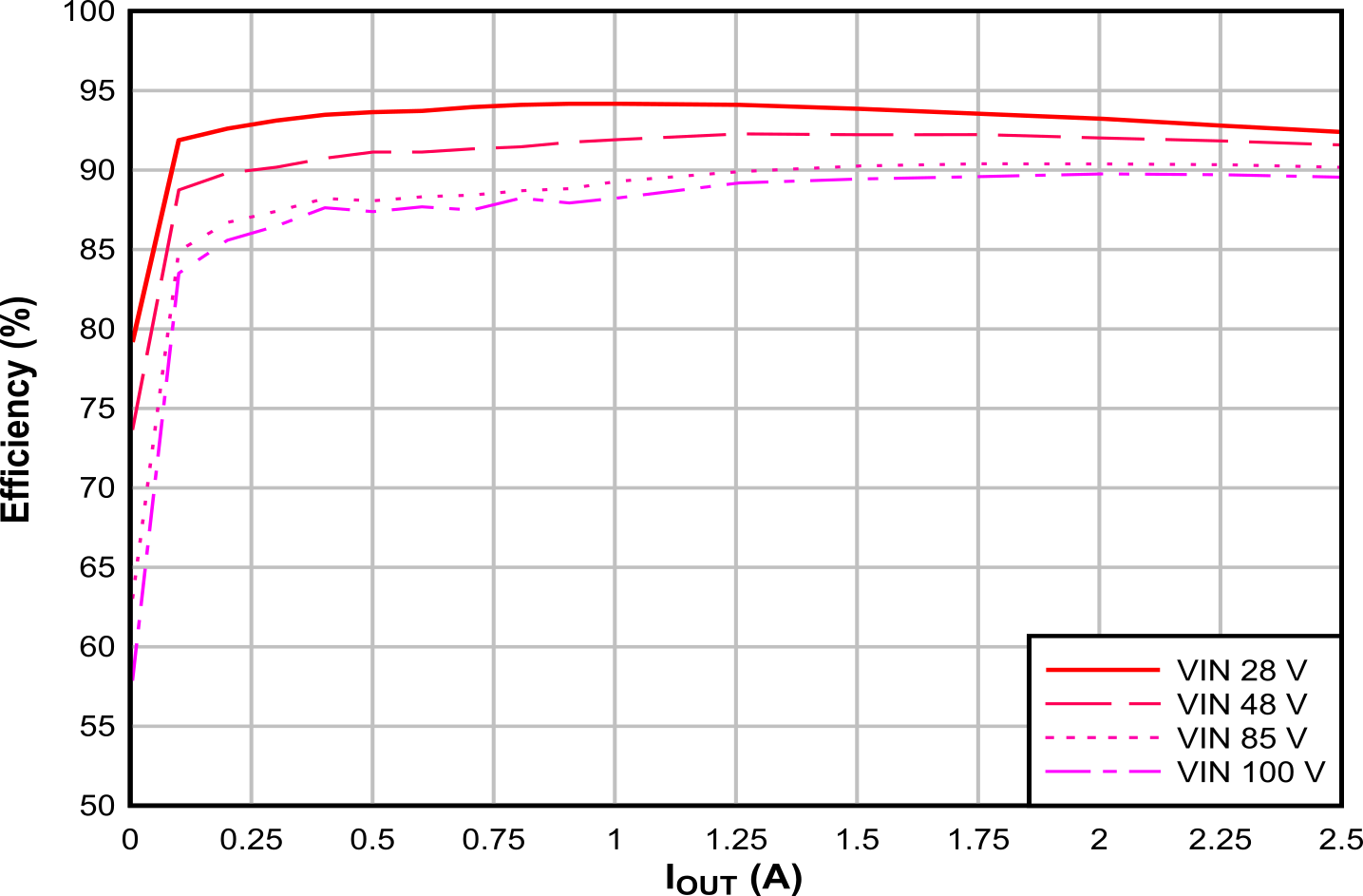
Typical Application, VIN(nom) = 48 V, VOUT = 12 V, IOUT(max) = 2.5 A, FSW(nom) = 300 kHz
GUID-BED486C2-A5F9-429D-B8F7-BF892CE6BC0F-low.pngTypical Application Efficiency, VOUT = 12 V