SNVS783K January 2012 – August 2021 LM5017
PRODUCTION DATA
- 1 Features
- 2 Applications
- 3 Description
- 4 Revision History
- 5 Pin Configuration and Functions
- 6 Specifications
-
7 Detailed Description
- 7.1 Overview
- 7.2 Functional Block Diagram
- 7.3
Feature Description
- 7.3.1 Control Overview
- 7.3.2 VCC Regulator
- 7.3.3 Regulation Comparator
- 7.3.4 Overvoltage Comparator
- 7.3.5 On-Time Generator
- 7.3.6 Current Limit
- 7.3.7 N-Channel Buck Switch and Driver
- 7.3.8 Synchronous Rectifier
- 7.3.9 Undervoltage Detector
- 7.3.10 Thermal Protection
- 7.3.11 Ripple Configuration
- 7.3.12 Soft-Start
- 7.4 Device Functional Modes
-
8 Application and Implementation
- 8.1 Application Information
- 8.2
Typical Application
- 8.2.1 Application Circuit: 12.5-V to 95-V Input and 10-V, 600-mA Output Buck Converter
- 8.2.2
Isolated DC/DC Converter Using LM5017
- 8.2.2.1 Design Requirements
- 8.2.2.2
Detailed Design Procedure
- 8.2.2.2.1 Transformer Turns Ratio
- 8.2.2.2.2 Total IOUT
- 8.2.2.2.3 RFB1, RFB2
- 8.2.2.2.4 Frequency Selection
- 8.2.2.2.5 Transformer Selection
- 8.2.2.2.6 Primary Output Capacitor
- 8.2.2.2.7 Secondary Output Capacitor
- 8.2.2.2.8 Type III Feedback Ripple Circuit
- 8.2.2.2.9 Secondary Diode
- 8.2.2.2.10 VCC and Boostrap Capacitor
- 8.2.2.2.11 Input Capacitor
- 8.2.2.2.12 UVLO Resistors
- 8.2.2.2.13 VCC Diode
- 8.2.2.3 Application Curves
- 9 Power Supply Recommendations
- 10Layout
- 11Device and Documentation Support
- 12Mechanical, Packaging, and Orderable Information
Package Options
Mechanical Data (Package|Pins)
Thermal pad, mechanical data (Package|Pins)
- DDA|8
Orderable Information
8.2.1.2.4 Inductor Selection
The minimum inductance is selected to limit the output ripple to 15 to 40 percent of the maximum load current. In addition, the peak inductor current at maximum load should be smaller than the minimum current limit as given in Section 6.5 table.
The inductor current ripple is given by Equation 13.
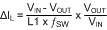
The maximum ripple is observed at maximum input voltage. Substituting VIN = 95 V and ΔIL = 40 percent × IOUT (max) results in L1 = 198 μH. The next higher standard value of 220 μH is chosen. The peak-to-peak minimum and maximum inductor current ripple are 40 mA and 181 mA at the minimum and maximum input voltages respectively. The peak inductor and switch current is given by Equation 14.
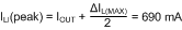
690 mA is less than the minimum current limit threshold of 0.7 A. The selected inductor should be able to withstand the maximum current limit of 1.3 A during startup and overload conditions without saturating.