SNVS783K January 2012 – August 2021 LM5017
PRODUCTION DATA
- 1 Features
- 2 Applications
- 3 Description
- 4 Revision History
- 5 Pin Configuration and Functions
- 6 Specifications
-
7 Detailed Description
- 7.1 Overview
- 7.2 Functional Block Diagram
- 7.3
Feature Description
- 7.3.1 Control Overview
- 7.3.2 VCC Regulator
- 7.3.3 Regulation Comparator
- 7.3.4 Overvoltage Comparator
- 7.3.5 On-Time Generator
- 7.3.6 Current Limit
- 7.3.7 N-Channel Buck Switch and Driver
- 7.3.8 Synchronous Rectifier
- 7.3.9 Undervoltage Detector
- 7.3.10 Thermal Protection
- 7.3.11 Ripple Configuration
- 7.3.12 Soft-Start
- 7.4 Device Functional Modes
-
8 Application and Implementation
- 8.1 Application Information
- 8.2
Typical Application
- 8.2.1 Application Circuit: 12.5-V to 95-V Input and 10-V, 600-mA Output Buck Converter
- 8.2.2
Isolated DC/DC Converter Using LM5017
- 8.2.2.1 Design Requirements
- 8.2.2.2
Detailed Design Procedure
- 8.2.2.2.1 Transformer Turns Ratio
- 8.2.2.2.2 Total IOUT
- 8.2.2.2.3 RFB1, RFB2
- 8.2.2.2.4 Frequency Selection
- 8.2.2.2.5 Transformer Selection
- 8.2.2.2.6 Primary Output Capacitor
- 8.2.2.2.7 Secondary Output Capacitor
- 8.2.2.2.8 Type III Feedback Ripple Circuit
- 8.2.2.2.9 Secondary Diode
- 8.2.2.2.10 VCC and Boostrap Capacitor
- 8.2.2.2.11 Input Capacitor
- 8.2.2.2.12 UVLO Resistors
- 8.2.2.2.13 VCC Diode
- 8.2.2.3 Application Curves
- 9 Power Supply Recommendations
- 10Layout
- 11Device and Documentation Support
- 12Mechanical, Packaging, and Orderable Information
Package Options
Mechanical Data (Package|Pins)
Thermal pad, mechanical data (Package|Pins)
- DDA|8
Orderable Information
8.2.2 Isolated DC/DC Converter Using LM5017
An isolated supply using the LM5017 is shown in Figure 8-5. Inductor (L) in a typical buck circuit is replaced with a coupled inductor (X1). A diode (D1) is used to rectify the voltage on a secondary output. The nominal voltage at the secondary output (VOUT2) is given by Equation 20.
Equation 20. 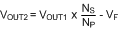
where
- VF is the forward voltage drop of D1
- NP and NS are the number of turns on the primary and secondary of coupled inductor X1.
For output voltage (VOUT1) more than one diode drop above the maximum VCC (8.55 V), the VCC pin can be diode connected to VOUT1 for higher efficiency and low dissipation in the IC. For a complete isolated bias design with LM5017, refer to the AN-2204 LM5017 Isolated Supply Evaluation Board application report.
 Figure 8-5 Typical Isolated Application Schematic