SNVS480J January 2007 – July 2020 LM5022
PRODUCTION DATA.
- 1 Features
- 2 Applications
- 3 Description
- 4 Revision History
- 5 Pin Configuration and Functions
- 6 Specifications
- 7 Detailed Description
-
8 Application and Implementation
- 8.1 Application Information
- 8.2
Typical Application
- 8.2.1 Design Requirements
- 8.2.2
Detailed Design Procedure
- 8.2.2.1 Switching Frequency
- 8.2.2.2 MOSFET
- 8.2.2.3 Output Diode
- 8.2.2.4 Boost Inductor
- 8.2.2.5 Output Capacitor
- 8.2.2.6 VCC Decoupling Capacitor
- 8.2.2.7 Input Capacitor
- 8.2.2.8 Current Sense Filter
- 8.2.2.9 RSNS, RS2, and Current Limit
- 8.2.2.10 Control Loop Compensation
- 8.2.2.11 Efficiency Calculations
- 8.2.3 Application Curves
- 9 Power Supply Recommendations
- 10Layout
- 11Device and Documentation Support
- 12Mechanical, Packaging, and Orderable Information
Package Options
Mechanical Data (Package|Pins)
- DGS|10
Thermal pad, mechanical data (Package|Pins)
Orderable Information
7.3.5 PWM Comparator and Slope Compensation
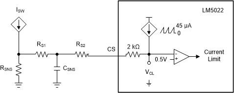
The PWM comparator compares the current ramp signal with the error voltage derived from the error amplifier output. The error amplifier output voltage at the COMP pin is offset by 1.4 V and then further attenuated by a 3:1 resistor divider. The PWM comparator polarity is such that 0 V on the COMP pin results in a zero duty cycle at the controller output. For duty cycles greater than 50%, current mode control circuits can experience subharmonic oscillation. By adding an additional fixed-slope voltage ramp signal (slope compensation), this oscillation can be avoided. Proper slope compensation damps the double pole associated with current mode control (see the Control Loop Compensation section) and eases the design of the control loop compensator. The LM5022 generates the slope compensation with a sawtooth-waveform current source with a slope of 45 µA × ƒSW, generated by the clock (see Figure 12). This current flows through an internal 2-kΩ resistor to create a minimum compensation ramp with a slope of 100 mV × ƒSW (typical). The slope of the compensation ramp increases when external resistance is added for filtering the current sense (RS1) or in the position RS2. As shown in Figure 12 and the Functional Block Diagram, the sensed current slope and the compensation slope add together to create the signal used for current limiting and for the control loop itself.
 Figure 12. Slope Compensation
 In peak current mode control, the optimal slope compensation is proportional to the slope of the inductor current during the power switch off-time. For boost converters, the inductor current slope while the MOSFET is off is (VO – VIN) / L. This relationship is combined with the requirements to set the peak current limit and is used to select RSNS and RS2 in the Application and Implementation section.