SNVS961E APRIL 2013 – January 2016 LM5023
PRODUCTION DATA.
- 1 Features
- 2 Applications
- 3 Description
- 4 Revision History
- 5 Pin Configuration and Functions
- 6 Specifications
-
7 Detailed Description
- 7.1 Overview
- 7.2 Functional Block Diagram
- 7.3 Feature Description
- 7.4 Device Functional Modes
- 8 Application and Implementation
- 9 Power Supply Recommendations
- 10Layout
- 11Device and Documentation Support
- 12Mechanical, Packaging, and Orderable Information
Package Options
Mechanical Data (Package|Pins)
- DGK|8
Thermal pad, mechanical data (Package|Pins)
Orderable Information
6 Specifications
6.1 Absolute Maximum Ratings
over operating free-air temperature range (unless otherwise noted)(1)(2)| MIN | MAX | UNIT | |||
|---|---|---|---|---|---|
| IQR | Negative injection current when the QR pin is being driven below ground | 4 | mA | ||
| VSD | Maximum voltage | –0.3 | 45 | V | |
| IVSD | VSD clamp continuous current | 500 | µA | ||
| VIN | Voltage range | SS, COMP, QR | –0.3 | 7 | V |
| CS | –0.3 | 1.25 | V | ||
| OUT | Gate-drive voltage at DRV | –0.3 | Self-limiting | V | |
| IOUT | Peak OUT current, source | 0.3 | A | ||
| IOUT | Peak OUT current sink | 0.7 | A | ||
| VCC | Bias supply voltage | –0.3 | 16 | V | |
| TJ | Operating junction temperature | –40 | 125 | ºC | |
| Tstg | Storage temperature | –55 | 150 | °C | |
(1) Stresses beyond those listed under may cause permanent damage to the device. These are stress ratings only, and functional operation of the device at these or any other conditions beyond those indicated under Recommended Operating Conditions is not implied. Exposure to absolute-maximum-rated conditions for extended periods may affect device reliability.
(2) The input negative-voltage and output voltage ratings may be exceeded if the input and output current ratings are observed.
6.2 ESD Ratings
| VALUE | UNIT | |||
|---|---|---|---|---|
| V(ESD) | Electrostatic discharge | Human-body model (HBM), per ANSI/ESDA/JEDEC JS-001(1) | ±2000 | V |
| Charged-device model (CDM), per JEDEC specification JESD22-C101(2) | ±1000 | V | ||
(1) JEDEC document JEP155 states that 500-V HBM allows safe manufacturing with a standard ESD control process.
(2) JEDEC document JEP157 states that 250-V CDM allows safe manufacturing with a standard ESD control process.
6.3 Recommended Operating Conditions
| MIN | MAX | UNIT | ||
|---|---|---|---|---|
| VCC | Bias supply voltage | 8 | 14 | V |
| IVSD | VSD Current | 2 | 100 | µA |
| IQR | QR pin current | 1 | 4 | mA |
| TJ | Junction temperature | –40 | 125 | ºC |
6.4 Thermal Information
| THERMAL METRIC(1) | LM5023 | UNIT | |
|---|---|---|---|
| DGK (VSSOP) | |||
| 8 PINS | |||
| RθJA | Junction-to-ambient thermal resistance | 168.6 | °C/W |
| RθJC(top) | Junction-to-case (top) thermal resistance | 59.6 | °C/W |
| RθJB | Junction-to-board thermal resistance | 88.8 | °C/W |
| ψJT | Junction-to-top characterization parameter | 7.1 | °C/W |
| ψJB | Junction-to-board characterization parameter | 87.5 | °C/W |
(1) For more information about traditional and new thermal metrics, see the Semiconductor and IC Package Thermal Metrics application report, SPRA953.
6.5 Electrical Characteristics
Minimum and maximum apply over the junction temperature range of –40 to +125°C. Minimum and maximum limits are specified through test, design, or statistical correlation. Typical values represent the most likely parametric norm at +25°C, and are provided for reference purposes only. Unless otherwise specified, the following conditions apply:VCC = 10 V, FSW = 100 kHz 50% duty cycle, no load on OUT.
| PARAMETER | TEST CONDITIONS | MIN | TYP | MAX | UNIT | |
|---|---|---|---|---|---|---|
| BIAS SUPPLY INPUT | ||||||
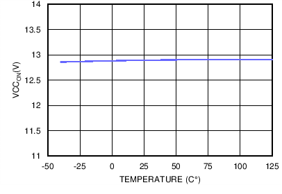
| VCCON | Controller enable threshold | 12 | 12.8 | 13.5 | V | |
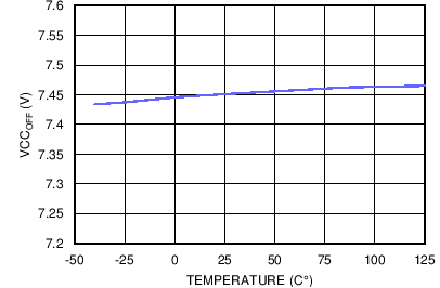
| VCCOFF | Minimum operating voltage | 7 | 7.5 | 8 | V | |
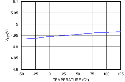
| VRST | Internal logic reset (fault latch) | VCC falling < VRST | 4.5 | 5 | 5.5 | V |
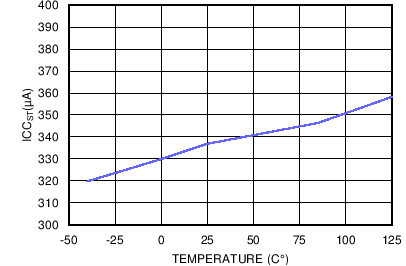
| ICCST | ICC current while in standby mode | COMP = 0.5 V, CS = 0 V, no switching | 340 | 420 | µA | |
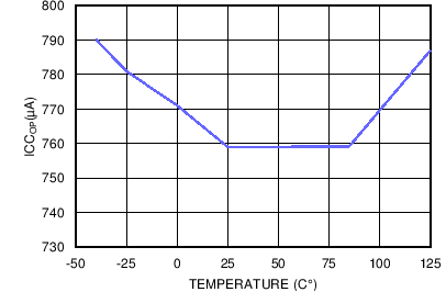
| ICCOP | Operating supply current | COMP = 2.25 V, OUT switching | 800 | µA | ||
| SHUTDOWN CONTROL (VSD PIN) | ||||||
| IVSD OFF | Off state leakage current | 0.1 | µA | |||
| VVSD ON1 | ON state pulldown voltage at 10 µA | After VCCON (IVSD = 10 µA) | 0.65 | V | ||
| VVSD_ON2 | ON state pulldown voltage at 100 µA | After VCCON (IVSD = 100 µA) | 0.84 | V | ||
| SKIP CYCLE MODE COMPARATOR | ||||||
| VSKIP | Skip cycle mode enable threshold | COMP falling | 70 | 120 | 170 | mV |
| VSK-HYS | Skip cycle mode hysteresis | 12 | mV | |||
| QR DETECT | ||||||
| VOVP | Overvoltage comparator threshold | 2.85 | 3 | 3.17 | V | |
| TOVP | Sample delay for OVP | 870 | 1050 | 1270 | ns | |
| VDEM | VDEM demagnetization threshold | 0.35 | V | |||
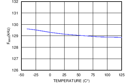
| FMAX | Maximum frequency | 114 | 130 | 148 | kHz | |
| TRST | TRESTART | 9.4 | 12 | 15.7 | µs | |
| PWM COMPARATORS | ||||||
| TPPWM | COMP to OUT propagation delay | COMP set to 2 V, CS stepped 0 to 0.4 V, time to OUT transition low, CLOAD = 0 | 20 | ns | ||
| DMIN | Minimum duty cycle | COMP = 0 V | 0% | |||
| GCOMP | COMP to PWM comparator gain | 0.33 | ||||
| VCOMP-O | COMP open circuit voltage | ICOMP = 20 µA | 4.3 | 4.9 | 5.8 | V |
| VCOMP-H | COMP at maximum VCS | 2.25 | V | |||
| ICOMP | COMP short circuit current | COMP = 0 V | –132 | µA | ||
| RCOMP | R pullup | 41 | 45 | 49 | kΩ | |
| CURRENT LIMIT | ||||||
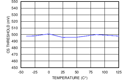
| VCS | Cycle-by-cycle sense voltage limit threshold | 450 | 500 | 550 | mV | |
| TLEB | Leading edge blanking time | 130 | ns | |||
| TPCS | Current limit to OUT delay | CS step from 0 to 0.6 V time to onset of OUT transition low, CLOAD = 0 | 22 | ns | ||
| RLEB | CS blanking sinking impedance | 15 | 35 | Ω | ||
| GCM | Current mirror gain | IQR = 2 mA | 100 | A/A | ||
| VFF | Line-current feedforward | IQR = 2 mA | 140 | mV | ||
| HICCUP MODE | ||||||
| TOL_10 | Over load detection timer | IVSD= 10 µA | 12 | ms | ||
| TOL_100 | Over load detection timer | IVSD= 100 µA | 1.2 | ms | ||
| OUTPUT GATE DRIVER | ||||||
| VOH | OUT high saturated | IOUT = 50 mA, VCC-OUT | 0.3 | 1.1 | V | |
| VOL | OUT low saturated | IOUT = 100 mA | 0.3 | 1 | V | |
| IPH | Peak OUT source current | OUT = VCC/2 | 0.3 | A | ||
| IPL | Peak OUT sink current | OUT = VCC/2 | 0.7 | A | ||
| tr | Rise time | CLOAD = 1 nF | 25 | ns | ||
| tf | Fall time | CLOAD = 1 nF | 15 | ns | ||
| SOFT-START | ||||||
| ISS | Soft-start current | 17 | 22 | 30 | µA | |
| THERMAL | ||||||
| TSD | Thermal shutdown temperature | 165 | ºC | |||
6.6 Typical Characteristics
