SNVS265C December 2003 – January 2016 LM5025
PRODUCTION DATA.
- 1 Features
- 2 Applications
- 3 Description
- 4 Revision History
- 5 Pin Configuration and Functions
- 6 Specifications
- 7 Detailed Description
- 8 Application and Implementation
- 9 Power Supply Recommendations
- 10Layout
- 11Device and Documentation Support
- 12Mechanical, Packaging, and Orderable Information
Package Options
Mechanical Data (Package|Pins)
Thermal pad, mechanical data (Package|Pins)
Orderable Information
8 Application and Implementation
NOTE
Information in the following applications sections is not part of the TI component specification, and TI does not warrant its accuracy or completeness. TI’s customers are responsible for determining suitability of components for their purposes. Customers must validate and test their design implementation to confirm system functionality.
8.1 Application Information
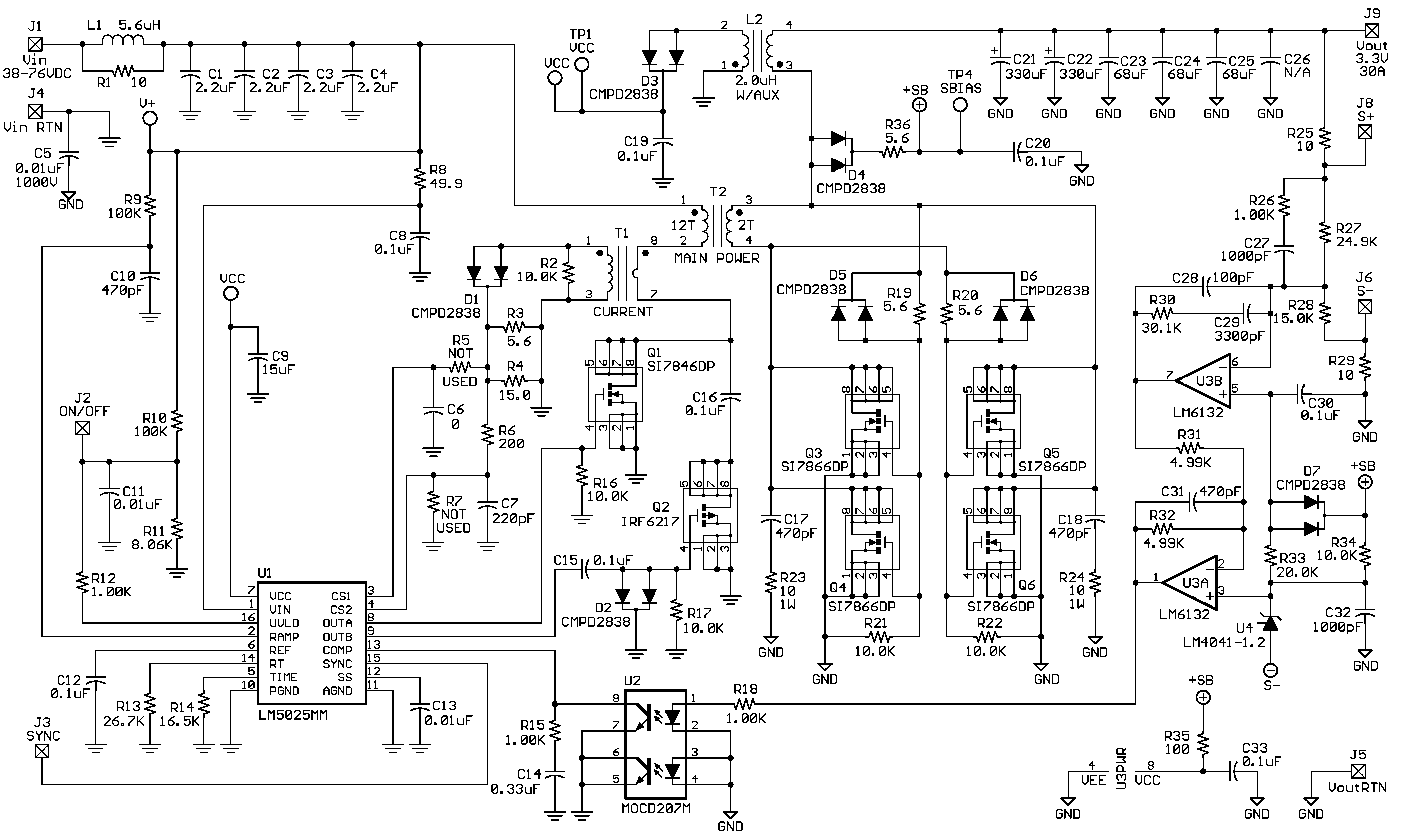
The LM5025 PWM controller contains all of the features necessary to implement power converters using the active clamp and reset technique. This section provides design guidance for a typical active clamp forward converter design. An actual application schematic of a 36-V to 78-V input, 3.3-V, 30-A output active clamp forward converter is also provided in Figure 21.
8.2 Typical Application
Figure 13 shows a simplified schematic of an active clamp forward power converter.
Power converters based on the forward topology offer high-efficiency and good power-handling capability in applications up to several hundred Watts. The operation of the transformer in a forward topology does not inherently self-reset each power switching cycle, a mechanism to reset the transformer is required. The active clamp reset mechanism is presently finding extensive use in medium-level power converters in the 50 W to
200 W range.
The forward converter is derived from the Buck topology family, employing a single modulating power switch. The main difference between the topologies is the forward topology employs a transformer to provide input and output ground isolation and a step down or step up function.
Each cycle, the main primary switch turns on and applies the input voltage across the primary winding. The transformer turns the voltage to a lower-level on the secondary side. The clamp capacitor along with the reset switch reverse biases the transformer primary each cycle when the main switch turns off. This reverse voltage resets the transformer. The clamp capacitor voltage is VIN / (1-D).
The secondary rectification employs self-driven synchronous rectification to maintain high-efficiency and ease of drive.
Feedback from the output is processed by an amplifier and reference, generating an error voltage, which is coupled back to the primary side control through an opto-coupler. The LM5025 voltage mode controller pulse width modulates the error signal with a ramp signal derived from the input voltage. Deriving the ramp signal slope from the input voltage provides line feed-forward, which improves line transient rejection. The LM5025 also provides a controlled delay necessary for the reset switch.
 Figure 13. Simplified Active Clamp Forward Power Converter
8.2.1 Design Requirements
This typical application provides an example of a fully-functional power converter based on the active clamp forward topology in an industry standard half-brick footprint.
The design requirements are:
- Input: 36 V to 78 V (100-V peak)
- Output Voltage: 3.3 V
- Output Current: 0 A to 30 A
- Measured Efficiency: 90.5% at 30 A, 92.5% at 15 A
- Frequency of Operation: 230 kHz
- Board Size: 2.3 × 2.4 × 0.5 inches
- Load Regulation: 1%
- Line Regulation: 0.1%
- Line UVLO, Hiccup Current Limit
8.2.2 Detailed Design Procedure
Before the controller design begins, the power stage design must be completed. This section describes the calculations needed to configure the LM5025 controller to meet the power stage design requirements.
8.2.2.1 Oscillator
The desired switching frequency F is set by a resistor connected between RT pin and ground. The resistance value RT is calculated from Equation 1:
where
- F is in kHz and RT in kΩ.
8.2.2.2 Soft-Start Ramp Time and Hiccup Interval
The soft-start ramp time and hiccup internal is programmed by a capacitor (CSS) on the SS pin to ground. The soft-start ramp time is determined by comparing the SS pin voltage with COMP pin voltage. When the SS voltage is less than COMP voltage, the COMP voltage is clamped by SS voltage. The PWM duty is limited by the clamped COMP voltage, so that soft-start can be achieved. The first PWM pulse is generated after COMP voltage reaches 1 V. So the soft-start ramp time of the output voltage can be estimated by Equation 2:

where
- VSS is the steady state COMP pin voltage. This voltage is determined by the output voltage, voltage divider, and the compensation network.
In hiccup mode, the SS current source is reduced to 1 µA. When the first PWM pulse is generated, the current source switches to 20 µA, and the power supply tries to start up again. The hiccup interval can be calculated by Equation 3:

8.2.2.3 Feed-Forward Ramp and Maximum On Time Clamp
An example illustrates the use of the Volt × Second Clamp comparator to achieve a 50% duty cycle limit, at 200 KHz, at a 48-V line input: A 50% duty cycle at a 200 KHz requires a 2.5 µs of ON time. At 48-V input the Volt × Second product is 120 V × µs (48 V × 2.5 µs). To achieve this clamp level, see Equation 4 and Equation 5:
Select CFF = 470 pF
RFF = 102 kΩ
The recommended capacitor value range for CFF is 100 pF to 1000 pF.
8.2.2.4 Dead Times
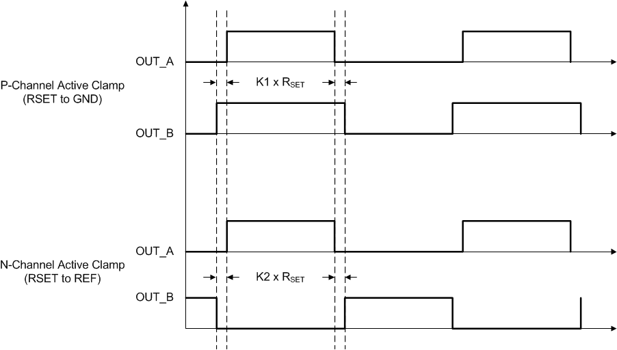
The magnitude of the overlap and dead time can be calculated as follows in Equation 6 and Equation 7:
where
- RSET in kΩ, Time in ns
 Figure 14. PWM Outputs
8.2.3 Application Curves

| Conditions: input voltage = 48 VDC, output current = 5 A | ||
| Trace 1: output voltage Volts/div = 0.5 V | ||
| Horizontal resolution = 1 ms/div | ||

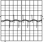
| Conditions: input voltage = 48 VDC, output current = 30 A | ||
| Bandwidth limit = 25 MHz | ||
| Trace 1: output ripple voltage Volts/div = 50 mV | ||
| Horizontal resolution = 2 μs/div |

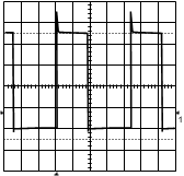
| Conditions: input voltage = 78 VDC, output current = 25 A | ||
| Trace 1: Q1 drain voltage Volts/div = 20 V | ||
| Horizontal resolution = 1 μs/div | ||

| Conditions: input voltage = 48 VDC, output current = 5 A to 25 A | ||
| Trace 1: output voltage Volts/div = 0.5 V | ||
| Trace 2: output current, Amps/div = 10 A | ||
| Horizontal resolution = 1 μs/div |

| Conditions: input voltage = 38 VDC, output current = 25 A | ||
| Trace 1: Q1 drain voltage Volts/div = 20 V | ||
| Horizontal resolution = 1 μs/div | ||

| Conditions: input voltage = 48 VDC, output current = 5 A | ||
| Synchronous rectifier, Q3 gate Volts/div = 5 V | ||
| Trace 1: synchronous rectifier, Q3 gate Volts/div = 5 V | ||
| Trace 2: synchronous rectifier, Q5 gate Volts/div = 5 V | ||
| Horizontal resolution = 1 μs/div |
8.2.4 System Example
Figure 21 shows an application circuit with 36-V to 78-V input and 3.3-V, 30-A output capability.
 Figure 21. Application Circuit