SNVS293F December 2004 – August 2016 LM5025A
PRODUCTION DATA.
- 1 Features
- 2 Applications
- 3 Description
- 4 Revision History
- 5 Pin Configuration and Functions
- 6 Specifications
- 7 Detailed Description
- 8 Application and Implementation
- 9 Power Supply Recommendations
- 10Layout
- 11Device and Documentation Support
- 12Mechanical, Packaging, and Orderable Information
Package Options
Mechanical Data (Package|Pins)
Thermal pad, mechanical data (Package|Pins)
Orderable Information
1 Features
- Internal Start-Up Bias Regulator
- 3-A Compound Main Gate Driver
- Programmable Line Undervoltage Lockout (UVLO) With Adjustable Hysteresis
- Voltage Mode Control With Feedforward
- Adjustable Dual Mode Overcurrent Protection
- Programmable Overlap or Dead Time Between the Main and Active Clamp Outputs
- Volt × Second Clamp
- Programmable Soft Start
- Leading Edge Blanking
- Single Resistor Programmable Oscillator
- Oscillator UP and DOWN Sync Capability
- Precision 5-V Reference
- Thermal Shutdown
- Packages:
- 16-Pin TSSOP
- Thermally Enhanced 16-Pin WSON
(5 mm × 5 mm)
2 Applications
- Server Power Supplies
- 48-V Telecom Power Supplies
- 42-V Automotive Applications
- High-Efficiency DC-to-DC Power Supplies
3 Description
The LM5025A is a functional variant of the LM5025 active clamp PWM controller. The functional differences of the LM5025A are that the CS1 and CS2 current limit thresholds have been increased to 0.5 V, the internal CS2 filter discharge device has been disabled and no longer operates each clock cycle, and the internal VCC and VREF regulators continue to operate when the line UVLO pin is below threshold.
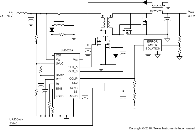
The LM5025A PWM controller contains all of the features necessary to implement power converters using the Active Clamp / Reset technique. With the active clamp technique, higher efficiencies and greater power densities can be realized compared to conventional catch winding or RDC clamp / reset techniques. Two control outputs are provided: the main power switch control (OUT_A) and the active clamp switch control (OUT_B). The two internal compound gate drivers parallel both MOS and bipolar devices, providing superior gate drive characteristics. This controller is designed for high-speed operation including an oscillator frequency range up to 1 MHz and total PWM and current sense propagation delays less than 100 ns. The LM5025A includes a high-voltage start-up regulator that operates over a wide input range of 13 V to 90 V. Additional features include: line undervoltage lockout (UVLO), soft start, oscillator UP and DOWN sync capability, precision reference, and thermal shutdown.
Device Information(1)
| PART NUMBER | PACKAGE | BODY SIZE (NOM) |
|---|---|---|
| LM5025A | TSSOP (16) | 5.00 mm × 4.40 mm |
| WSON (16) | 5.00 mm × 5.00 mm |
- For all available packages, see the orderable addendum at the end of the data sheet.
Simplified Active Clamp Forward Power Converter
