SNVS181C April 2004 – August 2016 LM5033
PRODUCTION DATA.
- 1 Features
- 2 Applications
- 3 Description
- 4 Revision History
- 5 Pin Configuration and Functions
- 6 Specifications
- 7 Detailed Description
- 8 Application and Implementation
- 9 Power Supply Recommendations
- 10Layout
- 11Device and Documentation Support
- 12Mechanical, Packaging, and Orderable Information
Package Options
Mechanical Data (Package|Pins)
Thermal pad, mechanical data (Package|Pins)
Orderable Information
8 Application and Implementation
NOTE
Information in the following applications sections is not part of the TI component specification, and TI does not warrant its accuracy or completeness. TI’s customers are responsible for determining suitability of components for their purposes. Customers should validate and test their design implementation to confirm system functionality.
8.1 Application Information
The following information is intended to provide guidelines for implementing the LM5033. However, final selection of all external components is dependent on the configuration and operating characteristics of the complete power conversion system.
8.2 Typical Application
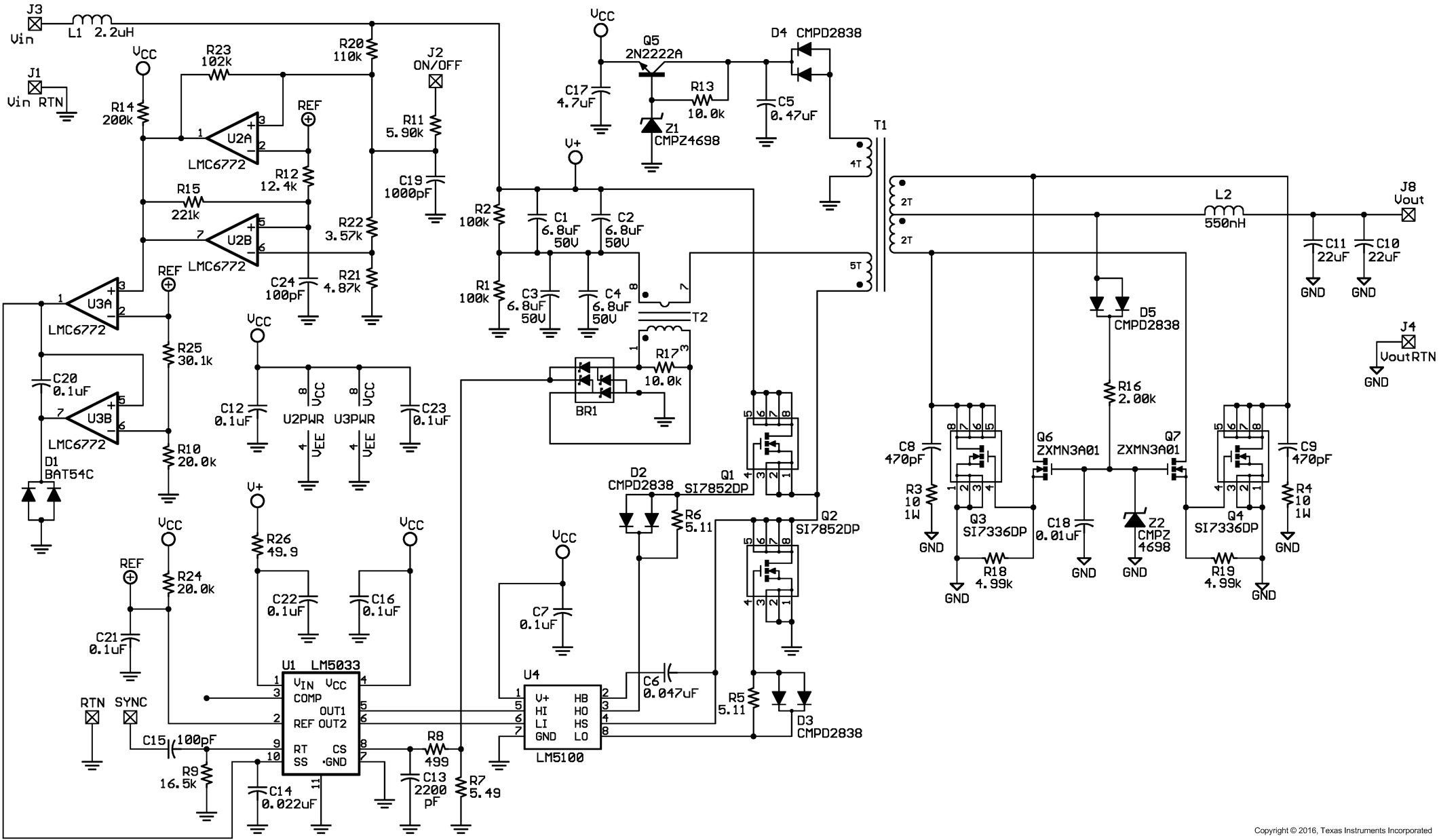
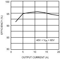
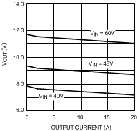
Figure 11 shows an example circuit for a half-bridge, 200-W, DC-DC converter built in a quarter brick format. The circuit is that of an intermediate bus converter (IBC) which operates open-loop (unregulated output), converting a nominal 48-V input to a nominal 9-V output with a 30-mΩ output impedance. The current sense transformer (T2), and the associated filter at the CS pin, provide overcurrent detection at approximately 23 A. The auxiliary winding on T1 powers VCC and the LM5100’s V+ pin (once the outputs are enabled) to reduce power dissipation within the LM5033. The LM5100 provides appropriate level shifting for Q1. Synchronous rectifiers Q3 and Q4 minimize conduction losses in the output stage. Dual comparators U2 and U3 provide undervoltage and overvoltage sensing at VIN. The undervoltage sense levels are 37 V increasing, and 33 V decreasing. The overvoltage sense levels are 63 V increasing, and 61.5 V decreasing. The circuit can be shut down by taking the ON/OFF input below 0.8 V. An external synchronizing frequency can be applied to the SYNC input. Measured efficiency and output characteristics for this circuit are shown in Figure 14 and Figure 15.
 Figure 11. Intermediate Bus Converter
40-V to 60-V Input; 7.5-V to 11.3-V, 20-A Output
8.2.1 Design Requirements
Table 1 lists the input parameters for this design example.
Table 1. Example Parameters
| PARAMETER | MIN | NOM | MAX | UNIT |
|---|---|---|---|---|
| Input voltage, VIN | 40 | 48 | 60 | V |
| Output voltage, VOUT | 7.5 | 9 | 11.3 | V |
| Output current, IOUT | 0 | 20 | A | |
| Output current limit, ILIMIT | 23 | A | ||
| Load regulation | ±4% | |||
| Oscillator frequency | 315 | kHz | ||
| Switching frequency | 157 | kHz |
8.2.2 Detailed Design Procedure
8.2.2.1 VIN
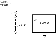
The voltage applied at VIN, normally the same as that applied to the primary of the main transformer, can be from 15 V to 90 V, with transient capability to 100 V. The current into VIN depends not only on VIN, but also on the load on the output driver pins, any load on VCC, and whether or not an external voltage is applied to VCC. If VIN is close to the absolute maximum rating of the LM5033, TI recommends the circuit of Figure 12 be used to filter transients which may occur at the input supply.
 Figure 12. Input Transient Protection
If VCC is not powered externally, requiring all internal bias currents for the LM5033, and output driver currents, to be supplied at VIN and through the internal regulator, the required input current (IIN) is shown in Figure 10.
If VCC is powered externally, IIN increases with VIN as shown in Figure 9 until the external voltage is applied to VCC. In most applications, this occurs once the outputs are enabled and load current begins to flow. The current into VIN then drops to a nominal 150 µA; SS is either open or grounded.
8.2.2.2 VCC
The capacitor at the VCC pin provides not only noise filtering and stability, but also a necessary time delay during start-up. The time delay allows the internal circuitry of the LM5033, and associated external circuitry, to stabilize before VCC reaches its final value, at which time the outputs are enabled and the soft-start sequence begins. Any external circuitry connected to the REF output and SS must be designed to stabilize during the time delay.
The current limit of the VCC regulator, and the external capacitor, determine the VCC turnon time delay. Typically, a 1-µF capacitor provides approximately 300 µs of delay, with larger capacitors providing proportionately longer delays. Experimentation with the final design may be necessary to determine the minimum value for the VCC capacitor.
8.2.2.3 Soft Start (SS)
The capacitor at SS determines the time required for the output duty cycle to increase from zero to the final value for regulation. The minimum acceptable time is dependent on the response of the feedback loops to the COMP pin, as well as the characteristics of the magnetic components. If the soft-start time is too quick, the system output could significantly overshoot its intended voltage before the loop is able to establish regulation, possibly adversely affecting the load. Experimentation with the final design is usually necessary to determine the minimum value for the SS capacitor.
8.2.2.4 Current Sense (CS)
This pin typically receives an input representative of the primary current from the current sense elements of the external circuitry. The peak amplitude at this pin must be less than 0.5 V for normal operation. Filtering at this pin must be sufficient to prevent false triggering of the current sense comparator, but not significantly delay detection of an overcurrent condition. The filter’s capacitor at CS must not be larger than 2200 pF.
8.2.2.5 Oscillator, Sync Input (RT/SYNC)
The internal oscillator frequency is generally selected in conjunction with the system magnetic components, and any other aspects of the system which may be affected by the frequency. The RT resistor at RT/SYNC sets the frequency according to Equation 2. Each output (OUT1 and OUT2) switches at half the oscillator frequency. If the required frequency value is critical in a particular application, the tolerance of the external resistor, and the frequency tolerance indicated in Electrical Characteristics, must be taken into account when selecting the resistor.
If the LM5033 is to be synchronized to an external clock, that signal must be coupled into RT/SYNC through a 100-pF capacitor. The RT resistor is still required in this case, and it must be selected to set the internal oscillator to a frequency lower than the external synchronizing frequency. The amplitude of the external pulses must take RT/SYNC above 3.8 V on the low-to-high transition but no higher than 5.5 V. The clock pulse width must be from 15 ns to 150 ns.
8.2.2.6 Deadtime Adjustment
TI recommends the circuits in Figure 13 if the application requires a change in the minimum deadtime between the outputs. Suggested values for the resistor and capacitor at each output are 500 Ω, and 100 pF, respectively for a nominal 50-ns change. The diodes can be 1N4148, or similar.
 Figure 13. Deadtime Adjustment
8.2.3 Application Curves
 Figure 14. Efficiency vs Output Current
 Figure 15. VOUT vs Load Current and VIN