SNVS181C April 2004 – August 2016 LM5033
PRODUCTION DATA.
- 1 Features
- 2 Applications
- 3 Description
- 4 Revision History
- 5 Pin Configuration and Functions
- 6 Specifications
- 7 Detailed Description
- 8 Application and Implementation
- 9 Power Supply Recommendations
- 10Layout
- 11Device and Documentation Support
- 12Mechanical, Packaging, and Orderable Information
Package Options
Mechanical Data (Package|Pins)
Thermal pad, mechanical data (Package|Pins)
Orderable Information
6 Specifications
6.1 Absolute Maximum Ratings
see (1)| MIN | MAX | UNIT | |
|---|---|---|---|
| VIN to GND | –0.3 | 100 | V |
| VCC to GND | –0.3 | 16 | V |
| RT/SYNC to GND | –0.3 | 5.5 | V |
| COMP, CS, and SS to GND | –0.3 | 7 | V |
| Power dissipation(2) | Internally Limited | ||
| Maximum junction temperature, TJ(MAX) | 150 | °C | |
| Storage temperature, Tstg | –65 | 150 | °C |
(1) Stresses beyond those listed under Absolute Maximum Ratings may cause permanent damage to the device. These are stress ratings only, which do not imply functional operation of the device at these or any other conditions beyond those indicated under Recommended Operating Conditions. Exposure to absolute-maximum-rated conditions for extended periods may affect device reliability.
(2) The maximum allowable power dissipation is a function of the maximum allowed junction temperature (TJ(max)), the ambient temperature (TA), and the junction-to-ambient thermal resistance (θJA). The maximum allowable power dissipation can be calculated from PD = (TJ(max) – TA) / θJA. Excessive power dissipation causes the thermal shutdown to activate.
6.2 ESD Ratings
| VALUE | UNIT | |||
|---|---|---|---|---|
| V(ESD) | Electrostatic discharge | Human-body model (HBM), per ANSI/ESDA/JEDEC JS-001(1) | ±2000 | V |
(1) JEDEC document JEP155 states that 500-V HBM allows safe manufacturing with a standard ESD control process.
6.3 Recommended Operating Conditions
over operating free-air temperature range (unless otherwise noted)| MIN | MAX | UNIT | ||
|---|---|---|---|---|
| VIN | Input voltage | 15 | 99 | V |
| TJ | Operating junction temperature | -40 | 125 | °C |
6.4 Thermal Information
| THERMAL METRIC(1) | LM5033 | UNIT | ||
|---|---|---|---|---|
| DGS (VSSOP) | DPR (WSON) | |||
| 10 PINS | 10 PINS | |||
| RθJA | Junction-to-ambient thermal resistance | 158 | 38.1 | °C/W |
| RθJC(top) | Junction-to-case (top) thermal resistance | 52.2 | 36.7 | °C/W |
| RθJB | Junction-to-board thermal resistance | 78.1 | 15.2 | °C/W |
| ψJT | Junction-to-top characterization parameter | 4.8 | 0.3 | °C/W |
| ψJB | Junction-to-board characterization parameter | 76.8 | 15.5 | °C/W |
| RθJC(bot) | Junction-to-case (bottom) thermal resistance | — | 4.7 | °C/W |
(1) For more information about traditional and new thermal metrics, see the Semiconductor and IC Package Thermal Metrics application report.
6.5 Electrical Characteristics
VIN = 48 V, VCC = 10 V (applied externally), and RT = 26.7 kΩ, Typical limits are given for TJ = 25°C, Minimum and Maximum limits apply over TJ = –40°C to 125°C (unless otherwise noted).(1)(2)| PARAMETER | TEST CONDITIONS | MIN | TYP | MAX | UNIT | |
|---|---|---|---|---|---|---|
| VCC STARTUP REGULATOR | ||||||
| VCCReg | VCC voltage | VCC is open | 9.2 | 9.6 | 10 | V |
| ICC(OUT) | VCC current limit | OUT1 and OUT2 disabled, extended supply to VCC disconnected | 20 | 34 | mA | |
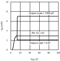
| IIN | Startup regulator current into VIN | Normal operation, VIN = 90 V | 150 | 500 | µA | |
| Extended VCC supply disconnected, output load = 1800 pF | 7 | mA | ||||
| VSS = 0 V | 3 | mA | ||||
| UVT | VCC undervoltage threshold (increasing VCC) | VCCReg – 300 mV | VCCReg – 100 mV | V | ||
| UVT hysteresis (decreasing VCC) | 2.3 | 2.8 | 3.3 | |||
| ICC(IN) | Supply current from external source to VCC | VSS = 0 V | 2 | 3 | mA | |
| SS is open, output load = 1800 pF | 7 | |||||
| 2.5-V REFERENCE | ||||||
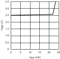
| VREF | Output voltage | REF sink current = 5 mA | 2.44 | 2.5 | 2.56 | V |
| Current sink capability | 5 | 13 | mA | |||
| CURRENT SENSE | ||||||
| CS | Threshold voltage | 0.45 | 0.5 | 0.55 | V | |
| CS delay to output | VCS taken from zero to 0.6 V, time for VOUT1 or VOUT2 to fall to 90% of VCC, CLOAD = 0 at OUT1 and OUT2 | 30 | ns | |||
| Current sink capability (clocked) | VCS ≤ 0.3 V | 3 | 6 | mA | ||
| SOFT START | ||||||
| Soft-start current source | 7 | 10 | 13 | µA | ||
| Soft-start to COMP offset | 0.25 | 0.5 | 0.75 | V | ||
| Open circuit voltage | 5 | V | ||||
| OSCILLATOR | ||||||
| FS1 | Internal frequency | RT = 26.7 kΩ | 175 | 200 | 225 | kHz |
| FS2 | Internal frequency | RT = 8.2 kΩ | 600 | kHz | ||
| VSYNC | Sync threshold | 3.2 | 3.8 | V | ||
| RT/SYNC DC voltage | 2 | V | ||||
| PWM COMPARATOR INPUT | ||||||
| tPWM | Gain from COMP to PWM comparator | 0.34 | V/V | |||
| Maximum duty cycle at OUT1 and OUT2 | See PWM Comparator | 100 × (0.5 tS – tD) / tS | % | |||
| Minimum duty cycle at OUT1 and OUT2 | VCOMP = 0 V | 0% | ||||
| Open circuit voltage | 4.2 | 5.2 | 6.2 | V | ||
| Short circuit current | VCOMP = 0 V | 0.6 | 1.1 | 1.5 | mA | |
| OUTPUT DRIVERS | ||||||
| tD | Deadtime | CLOAD = 0 at OUT1 and OUT2, time measured from 10% of falling output to 10% of rising output | 85 | 135 | 185 | ns |
| Rise time | CLOAD = 1 nF | 16 | ns | |||
| Fall time | CLOAD = 1 nF | 16 | ns | |||
| Output high voltage | IOUT = 50 mA (source) | VCC – 0.75 | VCC – 0.25 | V | ||
| Output low voltage | IOUT = 100 mA (sink) | 0.25 | 0.75 | V | ||
| Maximum source current | 1.5 | A | ||||
| Maximum sink current | 1.5 | A | ||||
| THERMAL SHUTDOWN | ||||||
| tSD | Shutdown temperature | 165 | °C | |||
| Shutdown temperature hysteresis | 15 | °C | ||||
(1) Minimum and maximum limits are 100% production tested at 25°C. Limits over the operating temperature range are specified through correlation using Statistical Quality Control (SQC) methods. Limits are used to calculate TI’s Average Outgoing Quality Level (AOQL).
(2) Typical specifications represent the most likely parametric norm at 25°C operation.
6.6 Typical Characteristics
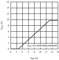
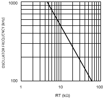
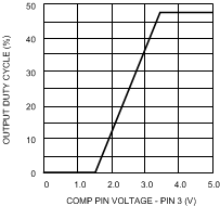
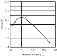 Figure 5. Soft-Start Current vs Temperature
| RT = 16.5 kΩ |
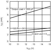
| VCC powered externally |
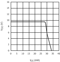
| VIN = 48 V |
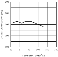
| RT = 26.7 kΩ |
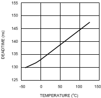 Figure 6. Dead Time vs Temperature
| VCC not powered externally |