SNVS631D January 2010 – October 2016 LM5035C
PRODUCTION DATA.
- 1 Features
- 2 Applications
- 3 Description
- 4 Revision History
- 5 Device Comparison Table
- 6 Pin Configuration and Functions
- 7 Specifications
-
8 Detailed Description
- 8.1 Overview
- 8.2 Functional Block Diagram
- 8.3
Feature Description
- 8.3.1 High-Voltage Start-Up Regulator
- 8.3.2 Line Undervoltage Detector
- 8.3.3 Line Overvoltage, Load Overvoltage, and Remote Thermal Protection
- 8.3.4 Reference
- 8.3.5 Cycle-by-Cycle Current Limit
- 8.3.6 Overload Protection Timer
- 8.3.7 Soft Start
- 8.3.8 PWM Comparator
- 8.3.9 Feedforward Ramp and Volt • Second Clamp
- 8.3.10 Oscillator, Sync Capability
- 8.3.11 Gate Driver Outputs (HO and LO)
- 8.3.12 Synchronous Rectifier Control Outputs (SR1 and SR2)
- 8.3.13 Thermal Protection
- 8.4 Device Functional Modes
- 9 Application and Implementation
- 10Power Supply Recommendations
- 11Layout
- 12Device and Documentation Support
- 13Mechanical, Packaging, and Orderable Information
Package Options
Mechanical Data (Package|Pins)
Thermal pad, mechanical data (Package|Pins)
- PWP|20
Orderable Information
8 Detailed Description
8.1 Overview
The LM5035C PWM controller contains all of the features necessary to implement half-bridge voltage-mode controlled power converters. The LM5035C provides two gate driver outputs to directly drive the primary side power MOSFETs and two signal level outputs to control secondary synchronous rectifiers through an isolation interface. Secondary side drivers, such as the LM5110, are typically used to provide the necessary gate drive current to control the sync MOSFETs. Synchronous rectification allows higher conversion efficiency and greater power density than conventional PN or Schottky rectifier techniques. The LM5035C can be configured to operate with bias voltages ranging from 8 V to 105 V. Additional features include line undervoltage lockout, cycle-by-cycle current limit, voltage feedforward compensation, hiccup mode fault protection with adjustable delays, soft start, a 2-MHz capable oscillator with synchronization capability, precision reference, thermal shutdown, and programmable volt•second clamping. These features simplify the design of voltage-mode half-bridge DC-DC power converters. See Functional Block Diagram.
8.2 Functional Block Diagram
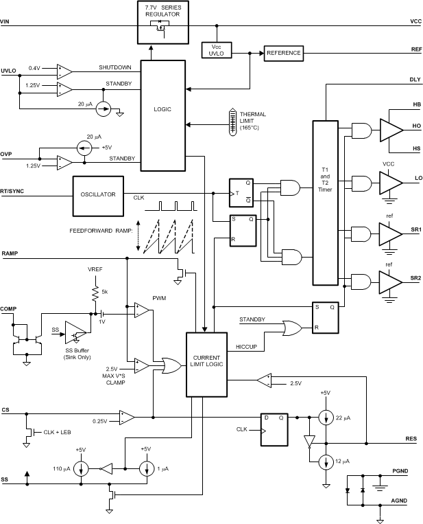
8.3 Feature Description
8.3.1 High-Voltage Start-Up Regulator
The LM5035C contains an internal high-voltage start-up regulator that allows the input pin (VIN) to be connected directly to a nominal 48-VDC input voltage. The regulator input can withstand transients up to 105 V. The regulator output at VCC (7.6 V) is internally current-limited to a minimum of 58 mA. When the UVLO pin potential is greater than 0.4 V, the VCC regulator is enabled to charge an external capacitor connected to the VCC pin. The VCC regulator provides power to the voltage reference (REF) and the output driver (LO). When the voltage on the VCC pin exceeds the UVLO threshold of 7.6 V, the internal voltage reference (REF) reaches its regulation setpoint of 5 V and the UVLO voltage is greater than 1.25 V, the controller outputs are enabled. The value of the VCC capacitor depends on the total system design, and its start-up characteristics. The recommended range of values for the VCC capacitor is 0.1 µF to 100 µF.
The VCC undervoltage comparator threshold is lowered to 6.2 V (typical) after VCC reaches the regulation setpoint. If VCC falls below this value, the outputs are disabled, and the soft-start capacitor is discharged. If VCC increases above 7.6 V, the outputs will be enabled and a soft-start sequence will commence.
The internal power dissipation of the LM5035C can be reduced by powering VCC from an external supply. In typical applications, an auxiliary transformer winding is connected through a diode to the VCC pin. This winding must raise the VCC voltage above 8.3 V to shut off the internal start-up regulator. Powering VCC from an auxiliary winding improves efficiency while reducing the controller’s power dissipation. The undervoltage comparator circuit will still function in this mode, requiring that VCC never falls below 6.2 V during the start-up sequence.
During a fault mode, when the converter auxiliary winding is inactive, external current draw on the VCC line should be limited such that the power dissipated in the start-up regulator does not exceed the maximum power dissipation of the IC package.
An external DC bias voltage can be used instead of the internal regulator by connecting the external bias voltage to both the VCC and the VIN pins. The external bias must be greater than 8.3 V to exceed the VCC UVLO threshold and less than the VCC maximum operating voltage rating (15 V).
8.3.2 Line Undervoltage Detector
The LM5035C contains a dual level undervoltage lockout (UVLO) circuit. When the UVLO pin voltage is below 0.4 V, the controller is in a low current shutdown mode. When the UVLO pin voltage is greater than 0.4 V but less than 1.25 V, the controller is in standby mode. In standby mode the VCC and REF bias regulators are active while the controller outputs are disabled. When the VCC and REF outputs exceed the VCC and REF undervoltage thresholds and the UVLO pin voltage is greater than 1.25 V, the outputs are enabled and normal operation begins. An external setpoint voltage divider from VIN to GND can be used to set the minimum operating voltage of the converter. The divider must be designed such that the voltage at the UVLO pin will be greater than 1.25 V when VIN enters the desired operating range. UVLO hysteresis is accomplished with an internal 23-µA current sink that is switched ON or OFF into the impedance of the setpoint divider. When the UVLO threshold is exceeded, the current sink is deactivated to quickly raise the voltage at the UVLO pin. When the UVLO pin voltage falls below the 1.25-V threshold, the current sink is enabled causing the voltage at the UVLO pin to quickly fall. The hysteresis of the 0.4-V shutdown comparator is internally fixed at 100 mV.
The UVLO pin can also be used to implement various remote enable and disable functions. See Soft Start for more details.
8.3.3 Line Overvoltage, Load Overvoltage, and Remote Thermal Protection
The LM5035C provides a multipurpose OVP pin that supports several fault protection functions. When the OVP pin voltage exceeds 1.25 V, the controller is held in standby mode, which immediately halts the PWM pulses at the HO and LO pins. In standby mode, the VCC and REF bias regulators are active while the controller outputs are disabled. When the OVP pin voltage falls below the 1.25-V OVP threshold, the outputs are enabled, and normal soft-start sequence begins. Hysteresis is accomplished with an internal 23-µA current source that is switched ON or OFF into the impedance of the OVP pin setpoint divider. When the OVP threshold is exceeded, the current source is enabled to quickly raise the voltage at the OVP pin. When the OVP pin voltage falls below the 1.25-V threshold, the current source is disabled causing the voltage at the OVP pin to quickly fall.
Several examples of the use of this pin are provided in Application Information.
8.3.4 Reference
The REF pin is the output of a 5-V linear regulator that can be used to bias an opto-coupler transistor and external housekeeping circuits. The regulator output is internally current limited to 15 mA (minimum).
8.3.5 Cycle-by-Cycle Current Limit
The CS pin is driven by a signal representative of the transformer primary current. If the voltage sensed at CS pin exceeds 0.25 V, the current sense comparator terminates the HO or LO output driver pulse. If the high current condition persists, the controller operates in a cycle-by-cycle current limit mode with duty cycle determined by the current sense comparator instead of the PWM comparator. Cycle-by-cycle current limiting may trigger the hiccup mode restart cycle depending on the configuration of the RES pin (see the following).
A small R-C filter connect to the CS pin and located near the controller is recommended to suppress noise. An internal 32-Ω MOSFET connected to the CS input discharges the external current sense filter capacitor at the conclusion of every cycle. The discharge MOSFET remains on for an additional 50 ns after the HO or LO driver switches high to blank leading edge transients in the current sensing circuit. Discharging the CS pin filter each cycle and blanking leading edge spikes reduces the filtering requirements and improves the current sense response time.
The current sense comparator is very fast and responds to short duration noise pulses. Layout considerations are critical for the current sense filter and sense resistor. The capacitor associated with the CS filter must be placed very close to the device and connected directly to the CS and AGND pins. If a current sense transformer is used, both leads of the transformer secondary should be routed to the filter network, which should be located close to the IC. If a sense resistor located in the source of the main MOSFET switch is used for current sensing, a low inductance type of resistor is required. When designing with a current sense resistor, all of the noise sensitive low power ground connections should be connected together near the AGND pin, and a single connection should be made to the power ground (sense resistor ground point).
8.3.6 Overload Protection Timer
The LM5035C provides a current limit restart timer to disable the outputs and force a delayed restart (hiccup mode) if a current limit condition is repeatedly sensed. The number of cycle-by-cycle current limit events required to trigger the restart is programmable by the external capacitor at the RES pin. During each PWM cycle, the LM5035C either sources or sinks current from the RES pin capacitor. If no current limit is detected during a cycle, a 12-µA discharge current sink is enabled to pull the RES pin to ground. If a current limit is detected, the 12-µA sink current is disabled and a 22-µA current source causes the voltage at the RES pin to gradually increase. The LM5035C protects the converter with cycle-by-cycle current limiting while the voltage at RES pin increases. If the RES voltage reaches the 2.5-V threshold, the following restart sequence occurs (also see Figure 11):
- The RES capacitor and SS capacitors are fully discharged
- The soft-start current source is reduced from 110 µA to 1 µA
- The SS capacitor voltage slowly increases. When the SS voltage reaches ≊1 V, the PWM comparator will produce the first narrow output pulse. After the first pulse occurs, the SS source current reverts to the normal 110-µA level. The SS voltage increases at its normal rate, gradually increasing the duty cycle of the output drivers
- If the overload condition persists after restart, cycle-by-cycle current limiting will begin to increase the voltage on the RES capacitor again, repeating the hiccup mode sequence
- If the overload condition no longer exists after restart, the RES pin will be held at ground by the 12-µA current sink and normal operation resumes
The overload timer function is very versatile and can be configured for the following modes of protection:
- Cycle-by-cycle only: The hiccup mode can be completely disabled by connecting a zero to 50-kΩ resistor from the RES pin to AGND. In this configuration, the cycle-by-cycle protection will limit the output current indefinitely and no hiccup sequences will occur.
- Hiccup only: The timer can be configured for immediate activation of a hiccup sequence upon detection of an overload by leaving the RES pin open circuit.
- Delayed Hiccup: Connecting a capacitor to the RES pin provides a programmed interval of cycle-by-cycle limiting before initiating a hiccup mode restart, as previously described. The dual advantages of this configuration are that a short term overload will not cause a hiccup mode restart but during extended overload conditions, the average dissipation of the power converter will be very low.
- Externally Controlled Hiccup: The RES pin can also be used as an input. By externally driving the pin to a level greater than the 2.5-V hiccup threshold, the controller will be forced into the delayed restart sequence. For example, the external trigger for a delayed restart sequence could come from an overtemperature protection circuit or an output overvoltage sensor.
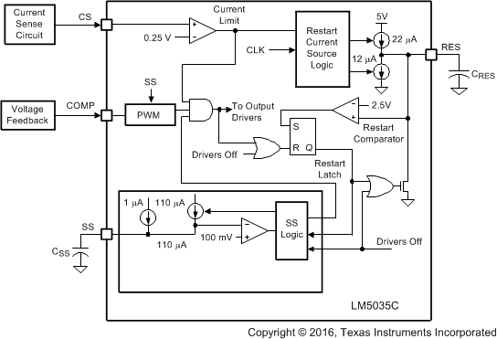 Figure 11. Current Limit Restart Circuit
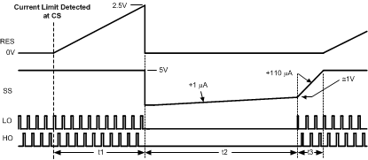 Figure 12. Current Limit Restart Timing
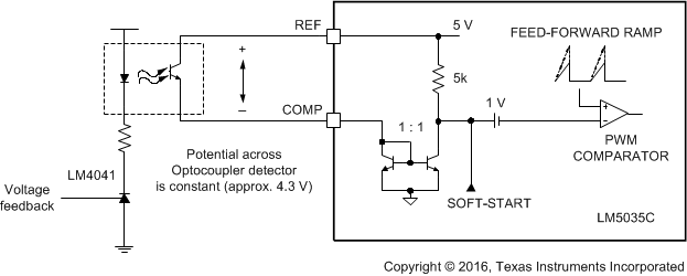 Figure 13. Optocoupler to COMP Interface
8.3.7 Soft Start
The soft-start circuit allows the regulator to gradually reach a steady state operating point, thereby reducing start-up stresses and current surges. When bias is supplied to the LM5035C, the SS pin capacitor is discharged by an internal MOSFET. When the UVLO, VCC and REF pins reach their operating thresholds, the SS capacitor is released and charged with a 110-µA current source. The PWM comparator control voltage is clamped to the SS pin voltage by an internal amplifier. When the PWM comparator input reaches 1 V, output pulses commence with slowly increasing duty cycle. The voltage at the SS pin eventually increases to 5 V, while the voltage at the PWM comparator increases to the value required for regulation as determined by the voltage feedback loop.
One method to shutdown the regulator is to ground the SS pin. This forces the internal PWM control signal to ground, reducing the output duty cycle quickly to zero. Releasing the SS pin begins a soft-start cycle and normal operation resumes. A second shutdown method is discussed in UVLO.
8.3.8 PWM Comparator
The pulse width modulation (PWM) comparator compares the voltage ramp signal at the RAMP pin to the loop error signal. This comparator is optimized for speed to achieve minimum controllable duty cycles. The loop error signal is received from the external feedback and isolation circuit is in the form of a control current into the COMP pin. The COMP pin current is internally mirrored by a matched pair of NPN transistors which sink current through a 5-kΩ resistor connected to the 5-V reference. The resulting control voltage passes through a 1-V level shift before being applied to the PWM comparator.
An opto-coupler detector can be connected between the REF pin and the COMP pin. Because the COMP pin is controlled by a current input, the potential difference across the optocoupler detector is nearly constant. The bandwidth limiting phase delay which is normally introduced by the significant capacitance of the opto-coupler is thereby greatly reduced. Higher loop bandwidths can be realized because the bandwidth-limiting pole associated with the opto-coupler is now at a much higher frequency. The PWM comparator polarity is configured such that with no current into the COMP pin, the controller produces the maximum duty cycle at the main gate driver outputs, HO and LO.
8.3.9 Feedforward Ramp and Volt • Second Clamp
An external resistor (RFF) and capacitor (CFF) connected to VIN, AGND, and the RAMP pin are required to create the PWM ramp signal. The slope of the signal at RAMP will vary in proportion to the input line voltage. This varying slope provides line feedforward information necessary to improve line transient response with voltage mode control. The RAMP signal is compared to the error signal by the pulse width modulator comparator to control the duty cycle of the HO and LO outputs. With a constant error signal, the on-time (TON) varies inversely with the input voltage (VIN) to stabilize the Volt • Second product of the transformer primary signal. The power path gain of conventional voltage-mode pulse width modulators (oscillator generated ramp) varies directly with input voltage. The use of a line generated ramp (input voltage feedforward) nearly eliminates this gain variation. As a result, the feedback loop is only required to make very small corrections for large changes in input voltage.
In addition to the PWM comparator, a Volt • Second Clamp comparator also monitors the RAMP pin. If the ramp amplitude exceeds the 2.5-V threshold of the Volt • Second Clamp comparator, the on-time is terminated. The CFF ramp capacitor is discharged by an internal 32-Ω discharge MOSFET controlled by the V•S Clamp comparator. If the RAMP signal does not exceed 2.5 V before the end of the clock period, then the internal clock will enable the discharge MOSFET to reset capacitor CFF.
By proper selection of RFF and CFF values, the maximum on-time of HO and LO can be set to the desired duration. The on-time set by the Volt • Second Clamp varies inversely to the line voltage because the RAMP capacitor is charged by a resistor (RFF) connected to VIN while the threshold of the clamp is a fixed voltage
(2.5 V). An example will illustrate the use of the Volt • Second Clamp comparator to achieve a 50% duty cycle limit at 200 kHz with a 48-V line input. A 50% duty cycle at a 200 kHz requires a 2.5-µs on-time. To achieve this maximum on-time clamp level, use Equation 1.

The recommended capacitor value range for CFF is 100 pF to 1000 pF. 470 pF is a standard value that can be paired with an 110 kΩ to approximate the desired 51.4-µs time constant. If load transient response is slowed by the 10% margin, the RFF value can be increased. The system signal-to-noise will be slightly decreased by increasing RFF × CFF.
8.3.10 Oscillator, Sync Capability
The LM5035C oscillator frequency is set by a single external resistor connected between the RT and AGND pins. To set a desired oscillator frequency, the necessary RT resistor is calculated from Equation 2.

For example, if the desired oscillator frequency is 400 kHz (HO and LO each switching at 200 kHz) a 15-kΩ resistor would be the nearest standard one percent value.
Each output (HO, LO, SR1 and SR2) switches at half the oscillator frequency. The voltage at the RT pin is internally regulated to a nominal 2 V. The RT resistor should be located as close as possible to the IC, and connected directly to the pins (RT and AGND). The tolerance of the external resistor, and the frequency tolerance indicated in Electrical Characteristics, must be considered when determining the worst-case frequency range.
The LM5035C can be synchronized to an external clock by applying a narrow pulse to the RT pin. The external clock must be at least 10% higher than the free-running oscillator frequency set by the RT resistor. If the external clock frequency is less than the RT resistor programmed frequency, the LM5035C will ignore the synchronizing pulses. The synchronization pulse width at the RT pin must be a minimum of 15 ns wide. The clock signal should be coupled into the RT pin through a 100-pF capacitor or a value small enough to ensure the pulse width at RT is less than 60% of the clock period under all conditions. When the synchronizing pulse transitions low-to-high (rising edge), the voltage at the RT pin must be driven to exceed 3.2 V from its nominal 2-VDC level. During the clock signal’s low time, the voltage at the RT pin will be clamped at 2 VDC by an internal regulator. The output impedance of the RT regulator is approximately 100 Ω. The RT resistor is always required, whether the oscillator is free running or externally synchronized.
8.3.11 Gate Driver Outputs (HO and LO)
The LM5035C provides two alternating gate driver outputs: the floating high-side gate driver HO and the ground referenced low-side driver LO. Each driver is capable of sourcing 1.25 A and sinking 2-A peak. The HO and LO outputs operate in an alternating manner, at one-half the internal oscillator frequency. The LO driver is powered directly by the VCC regulator. The HO gate driver is powered from a bootstrap capacitor connected between HB and HS. An external diode connected between VCC (anode pin) and HB (cathode pin) provides the high-side gate driver power by charging the bootstrap capacitor from VCC when the switch node (HS pin) is low. When the high-side MOSFET is turned on, HB rises to a peak voltage equal to VVCC + VHS where VHS is the switch node voltage.
The HB and VCC capacitors should be placed close to the pins of the LM5035C to minimize voltage transients due to parasitic inductances since the peak current sourced to the MOSFET gates can exceed 1.25 A. The recommended value of the HB capacitor is 0.01 µF or greater. A low ESR or ESL capacitor, such as a surface mount ceramic, should be used to prevent voltage droop during the HO transitions.
The maximum duty cycle for each output is equal to or slightly less than 50% due to any programmed sync rectifier delay. The programmed sync rectifier delay is determined by the DLY pin resistor. If the COMP pin is open circuit, the outputs will operate at maximum duty cycle. The maximum duty cycle for each output can be calculated with Equation 3.

where
- TS is the period of one complete cycle for either the HO or LO outputs
- T1 is the programmed sync rectifier delay
For example, if the oscillator frequency is 200 kHz, each output will cycle at 100 kHz (TS = 10 µs). Using no programmed delay, the maximum duty cycle at this frequency is calculated to be 50%. Using a programmed sync rectifier delay of 100 ns, the maximum duty cycle is reduced to 49%. Because there is no fixed dead time in the LM5035C, TI recommends that the delay pin resistor not be less than 10 K. Internal delays, which are not ensured, are the only protection against cross conduction if the programmed delay is zero, or very small.
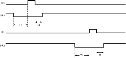 Figure 14. HO, LO, SR1, and SR2 Timing Diagram
8.3.12 Synchronous Rectifier Control Outputs (SR1 and SR2)
Synchronous rectification (SR) of the transformer secondary provides higher efficiency, especially for low-output voltage converters. The reduction of rectifier forward voltage drop (0.5 V – 1.5 V) to 10 mV – 200 mV VDS voltage for a MOSFET significantly reduces rectification losses. In a typical application, the transformer secondary winding is center tapped, with the output power inductor in series with the center tap. The SR MOSFETs provide the ground path for the energized secondary winding and the inductor current. Figure 14 shows that the SR2 MOSFET is conducting while HO enables power transfer from the primary. The SR1 MOSFET must be disabled during this period since the secondary winding connected to the SR1 MOSFET drain is twice the voltage of the center tap. At the conclusion of the HO pulse, the inductor current continues to flow through the SR1 MOSFET body diode. Because the body diode causes more loss than the SR MOSFET, efficiency can be improved by minimizing the T2 period while maintaining sufficient timing margin over all conditions (component tolerances, and so forth) to prevent shoot-through current. When LO enables power transfer from the primary, the SR1 MOSFET is enabled and the SR2 MOSFET is off.
During the time that neither HO nor LO is active, the inductor current is shared between both the SR1 and SR2 MOSFETs which effectively shorts the transformer secondary and cancels the inductance in the windings. The SR2 MOSFET is disabled before LO delivers power to the secondary to prevent power being shunted to ground. The SR2 MOSFET body diode continues to carry about half the inductor current until the primary power raises the SR2 MOSFET drain voltage and reverse biases the body diode. Ideally, dead-time T1 would be set to the minimum time that allows the SR MOSFET to turn off before the SR MOSFET body diode starts conducting.
The SR1 and SR2 outputs are powered directly by the 5-V reference regulator. Each output is capable of sourcing 0.09 A and sinking 0.2-A peak. The SR1 and SR2 signals can control SR MOSFET gate drivers through a digital isolator. The actual gate sourcing and sinking currents are provided by the secondary-side bias supply and gate drivers.
The timing of SR1 and SR2 with respect to HO and LO is shown in Figure 14. SR1 is configured out of phase with HO and SR2 is configured out of phase with LO. The dead time between transitions is programmable by a resistor connected from the DLY pin to the AGND pin. Typically, RDLY is set in the range of 10 kΩ to 100 kΩ. The dead-time periods can be calculated using Equation 4 and Equation 5.
When UVLO falls below 1.25 V, or during hiccup current limit, both SR1 and SR2 are held low. During normal operation, if soft start is held low, both SR1 and SR2 will be high.
8.3.13 Thermal Protection
Internal thermal shutdown circuitry is provided to protect the integrated circuit in the event the maximum rated junction temperature is exceeded. When activated, typically at 165°C, the controller is forced into a low-power standby state with the output drivers (HO, LO, SR1, and SR2), the bias regulators (VCC and REF) disabled. This helps to prevent catastrophic failures from accidental device overheating. During thermal shutdown, the soft-start capacitor is fully discharged and the controller follows a normal start-up sequence after the junction temperature falls to the operating level (145°C).
8.4 Device Functional Modes
The LM5035C can be used as a half-bridge PWM controller or as a push-pull PWM controller. To implement the LM5035C in a push-pull application, the HB pin is connected to VCC and the HS pin is connected to PGND. The LM5035C will deliver 180º out-of-phase ground-referenced PWM signals to the gates of the power MOSFETS. The high-side driver has an HS-to-GND maximum voltage rating of 105 V, but in higher-voltage applications the high-side MOSFET can be driven with a gate-drive transformer.