SNVS628H October 2009 – December 2019 LM5060
PRODUCTION DATA.
- 1 Features
- 2 Applications
- 3 Description
- 4 Revision History
- 5 Pin Configuration and Functions
- 6 Specifications
- 7 Detailed Description
-
8 Application and Implementation
- 8.1 Application Information
- 8.2
Typical Applications
- 8.2.1
Example Number 1: LM5060EVAL Design
- 8.2.1.1 Design Requirements
- 8.2.1.2
Detailed Design Procedure
- 8.2.1.2.1 VDS Fault Detection and Selecting Sense Pin Resistor RS
- 8.2.1.2.2 Turn-On Time
- 8.2.1.2.3 Fault Detection Delay Time
- 8.2.1.2.4 MOSFET Selection
- 8.2.1.2.5 Input and Output Capacitors
- 8.2.1.2.6 UVLO, OVP
- 8.2.1.2.7 POWER GOOD Indicator
- 8.2.1.2.8 Input Bypass Capacitor
- 8.2.1.2.9 Large Load Capacitance
- 8.2.1.3 Application Curves
- 8.2.2 Example Number 2: Reverse Polarity Protection With Diodes
- 8.2.3 Example Number 3: Reverse Polarity Protection With Resistor
- 8.2.1
Example Number 1: LM5060EVAL Design
- 9 Power Supply Recommendations
- 10Layout
- 11Device and Documentation Support
- 12Mechanical, Packaging, and Orderable Information
Package Options
Mechanical Data (Package|Pins)
- DGS|10
Thermal pad, mechanical data (Package|Pins)
Orderable Information
7.4.2 Status Conditions
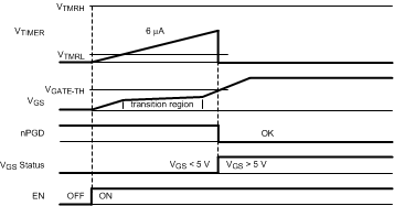
Output responses of the LM5060 to various input conditions is shown in Table 1. The input parameters include Enable (EN), UVLO, OVP, input voltage (VIN), Start-Up Fault (VGS) and Run Fault (VDS) conditions. The output responses are the VIN pin current consumption, the GATE charge current, the TIMER capacitor charge (or discharge) current, the GATE discharge current if the timer capacitor voltage has reached the VTMRH threshold (typically 2 V), as well as the status of nPGD.
 Figure 21. Voltages During Normal Start Up Sequence
 Table 1. Overview of Operating Conditions
| INPUTS | OUTPUTS | STATUS | |||||||||
|---|---|---|---|---|---|---|---|---|---|---|---|
| EN | UVLO | OVP
(typ) |
VIN
(typ) |
SENSE-OUT | GATE-OUT | VIN Current
(typ) |
GATE Current
(typ) |
TIMER | GATE after
TIMER > 2 V |
nPGD | |
| L | L | – | >5.10 V | – | – | 0.009 mA | 2.2 mA sink | Low | – | – | Disabled |
| L | H | – | >5.10 V | – | – | 0.009 mA | 2.2 mA sink | Low | – | – | Disabled |
| H | L | <2 V | >5.10 V | SENSE>OUT | – | 0.56 mA | 2.2 mA sink | Low | – | H | Standby |
| SENSE<OUT | L | ||||||||||
| H | L | >2 V | >5.10 V | SENSE>OUT | – | 0.56 mA | 80 mA sink | Low | – | H | Standby |
| SENSE<OUT | L | ||||||||||
| H | H | <2 V | >5.10 V | SENSE>OUT | <5 V | 1.4 mA | 24-µA source | 6-µA source | 80 mA sink | H | Enabled |
| SENSE<OUT | Low | – | L | ||||||||
| H | H | <2 V | >5.10 V | SENSE>OUT | >5 V | 1.4 mA | 24-µA source | 11-µA source | 80 mA sink | H | Enabled |
| SENSE<OUT | Low | – | L | ||||||||
| H | H | >2 V | >5.10 V | SENSE>OUT | – | 1.4 mA | 80 mA sink | Low | – | H | Over-voltage |
| SENSE<OUT | L | ||||||||||
| H | H | <2 V | <5.10 V | – | – | 1.4 mA | 2.2 mA sink
(see (1)) |
Low | – | H | Power on reset |
(1) The 2.2 mA sink current is valid for with the VIN pin ≥ 5.1 V. When the VIN pin < 5.1 V the sink current is lower. See ‘GATE Pin Off Current vs. VIN’ plot inTypical Characteristics.