SNVS600J December 2008 – June 2022 LM5088 , LM5088-Q1
PRODUCTION DATA
- 1 Features
- 2 Applications
- 3 Description
- 4 Revision History
- 5 Pin Configuration and Functions
- 6 Specifications
-
7 Detailed Description
- 7.1 Overview
- 7.2 Functional Block Diagram
- 7.3
Feature Description
- 7.3.1 High Voltage Low-Dropout Regulator
- 7.3.2 Line Undervoltage Detector
- 7.3.3 Oscillator and Sync Capability
- 7.3.4 Error Amplifier and PWM Comparator
- 7.3.5 Ramp Generator
- 7.3.6 Dropout Voltage Reduction
- 7.3.7 Frequency Dithering (LM5088-1 Only)
- 7.3.8 Cycle-by-Cycle Current Limit
- 7.3.9 Overload Protection Timer (LM5088-2 Only)
- 7.3.10 Soft Start
- 7.3.11 HG Output
- 7.3.12 Thermal Protection
- 7.4 Device Functional Modes
-
8 Application and Implementation
- 8.1 Application Information
- 8.2
Typical Application
- 8.2.1 Design Requirements
- 8.2.2
Detailed Design Procedure
- 8.2.2.1 Timing Resistor
- 8.2.2.2 Output Inductor
- 8.2.2.3 Current Sense Resistor
- 8.2.2.4 Ramp Capacitor
- 8.2.2.5 Output Capacitors
- 8.2.2.6 Input Capacitors
- 8.2.2.7 VCC Capacitor
- 8.2.2.8 Bootstrap Capacitor
- 8.2.2.9 Soft-Start Capacitor
- 8.2.2.10 Output Voltage Divider
- 8.2.2.11 UVLO Divider
- 8.2.2.12 Restart Capacitor (LM5008-2 Only)
- 8.2.2.13 MOSFET Selection
- 8.2.2.14 Diode Selection
- 8.2.2.15 Snubber Components Selection
- 8.2.2.16 Error Amplifier Compensation
- 8.2.3 Application Curves
- 9 Power Supply Recommendations
- 10Layout
- 11Device and Documentation Support
- 12Mechanical, Packaging, and Orderable Information
Package Options
Mechanical Data (Package|Pins)
- PWP|16
Thermal pad, mechanical data (Package|Pins)
- PWP|16
Orderable Information
7.3.9 Overload Protection Timer (LM5088-2 Only)
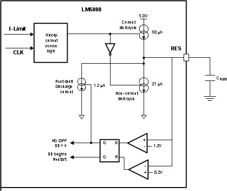
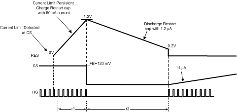
To further protect the external circuitry during a prolonged over current condition, the LM5088-2 provides a current limit timer to disable the switching regulator and provide a delay before restarting (hiccup mode). The number of current limit events required to trigger the restart mode is programmed by an external capacitor at the RES pin. During each PWM cycle, as shown in Figure 7-8, the LM5088 either sinks current from or sources current into the RES capacitor. If the emulated current ramp exceeds the 1.2-V current limit threshold, the present PWM cycle is terminated and the LM5088 sources 50 µA into the RES pin capacitor during the next PWM clock cycle. If a current limit event is not detected in a given PWM cycle, the LM5088 disables the 50-µA source current and sinks 27 µA from the RES pin capacitor during the next cycle. In an overload condition, the LM5088 protects the converter with cycle-by-cycle current limiting until the voltage at RES pin reaches 1.2 V. When RES reaches 1.2 V, a hiccup mode sequence is initiated as follows:
- The SS capacitor is fully discharged.
- The RES capacitor is discharged with 1.2 µA
- Once the RES capacitor reaches 0.2 V, a normal soft-start sequence begins. This provides a time delay before restart.
- If the overload condition persists after restart, the cycle repeats.
- If the overload condition no longer exists after restart, the RES pin is held at ground by the 27-µA discharge current source and normal operation resumes.
The overload protection timer is very versatile and can be configured for the following modes of protection:
- Cycle-by-Cycle only: The hiccup mode can be completely disabled by connecting the RES pin to GND. In this configuration, the cycle-by-cycle protection limits the output current indefinitely and no hiccup sequence occurs.
- Delayed Hiccup: Connecting a capacitor to the RES pin provides a programmed number of cycle-by-cycle current limit events before initiating a hiccup mode restart, as previously described. The advantage of this configuration is that a short term overload does not cause a hiccup mode restart but during extended overload conditions, the average dissipation of the power converter is very low.
- Externally Controlled Hiccup: The RES pin can also be used as an input. By externally driving the pin to a level greater than the 1.2-V hiccup threshold, the controller is forced into the delayed restart sequence. For example, the external trigger for a delayed restart sequence could come from an overtemperature protection or an output overvoltage sensor.
 Figure 7-7 Current Limit Restart Circuit
 Figure 7-8 Current Limit Restart Timing Diagram