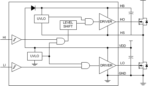
The LM5100A/B/C and LM5101A/B/C high-voltage gate drivers are designed to drive both the high-side and the low-side N-Channel MOSFETs in a synchronous buck or a half-bridge configuration. The floating high-side driver is capable of operating with supply voltages up to 100 V. The A versions provide a full 3-A of gate drive, while the B and C versions provide 2 A and 1 A, respectively. The outputs are independently controlled with CMOS input thresholds (LM5100A/B/C) or TTL input thresholds
(LM5101A/B/C).
An integrated high-voltage diode is provided to charge the high-side gate drive bootstrap capacitor. A robust level shifter operates at high speed while consuming low power and providing clean level transitions from the control logic to the high-side gate driver. Undervoltage lockout is provided on both the low-side and the high-side power rails. These devices are available in the standard SOIC-8 pin, SO PowerPAD-8 pin, and the WSON-10 pin packages. The LM5100C and LM5101C are also available in MSOP-PowerPAD-8 package. The LM5101A is also available in WSON-8 pin package.
PART NUMBER | INPUT THRESHOLD | PEAK OUTPUT CURRENT |
---|---|---|
LM5100A | CMOS | 3 A |
LM5101A | TTL | 3 A |
LM5100B | CMOS | 2 A |
LM5101B | TTL | 2 A |
LM5100C | CMOS | 1 A |
LM5101C | TTL | 1 A |
Changes from P Revision (March 2013) to Q Revision
Changes from O Revision (March 2013) to P Revision
PART NUMBER | PACKAGE | BODY SIZE (NOM) |
---|---|---|
LM5100A, LM5100C | WSON (10) | 4.00 mm × 4.00 mm |
SO PowerPAD™ (8) | 3.90 mm × 4.89 mm | |
SOIC (8) | 3.91 mm × 4.90 mm | |
LM5100B, LM5101B | WSON (10) | 4.00 mm × 4.00 mm |
SOIC (8) | 3.91 mm × 4.90 mm | |
LM5101A | WSON (8) | 4.00 mm × 4.00 mm |
WSON (10) | 4 .00mm × 4.00 mm | |
SO PowerPAD (8) | 3.90 mm × 4.89 mm | |
SOIC (8) | 3.91 mm × 4.90 mm | |
LM5101C | MSOP PowerPAD (8) | 3.00 mm × 3.00 mm |
WSON (10) | 4.00 mm × 4.00 mm | |
SOIC (8) | 3.91 mm × 4.90 mm |
PIN | I/O | DESCRIPTION | ||||
---|---|---|---|---|---|---|
NAME | 8 PINS | 10 PINS(1) | ||||
HB | 2 | 2 | I | High-side gate driver bootstrap supply. Connect the positive terminal of the bootstrap capacitor to HB and the negative terminal to HS. The bootstrap capacitor should be placed as close to the IC as possible. | ||
HI | 5 | 7 | I | High-side driver control input. The LM5100A/B/C inputs have CMOS type thresholds. The LM5101A/B/C inputs have TTL type thresholds. Unused inputs should be tied to ground and not left open. | ||
HO | 3 | 3 | O | High-side gate driver output. Connect to the gate of high-side MOSFET with a short, low inductance path. | ||
HS | 4 | 4 | — | High-side MOSFET source connection. Connect to the bootstrap capacitor negative terminal and the source of the high-side MOSFET. | ||
LI | 6 | 8 | I | Low-side driver control input. The LM5100A/B/C inputs have CMOS type thresholds. The LM5101A/B/C inputs have TTL type thresholds. Unused inputs should be tied to ground and not left open. | ||
LO | 8 | 10 | O | Low-side gate driver output. Connect to the gate of the low-side MOSFET with a short, low inductance path. | ||
VDD | 1 | 1 | I | Positive gate drive supply . Locally decouple to VSS using low ESR/ESL capacitor located as close to the IC as possible. | ||
VSS | 7 | 9 | — | Ground return. All signals are referenced to this ground. | ||
EP(2) | — | TI recommends that the exposed pad on the bottom of the package is soldered to ground plane on the PC board, and that ground plane should extend out from beneath the IC to help dissipate heat. |
MIN | MAX | UNIT | |
---|---|---|---|
VDD to VSS | −0.3 | 18 | V |
HB to HS | −0.3 | 18 | V |
LI or HI input | −0.3 | VDD + 0.3 | V |
LO output | −0.3 | VDD + 0.3 | V |
HO output | VHS − 0.3 | VHB + 0.3 | V |
HS to VSS (3) | −5 | 100 | V |
HB to VSS | 118 | V | |
Junction temperature | 150 | °C | |
Storage temperature | −55 | 150 | °C |
VALUE | UNIT | ||||
---|---|---|---|---|---|
V(ESD) | Electrostatic discharge | Human-body model (HBM), per ANSI/ESDA/JEDEC JS-001(1) | ±2000 | V | |
Machine Model (MM) (2) | Option A | 50 | |||
Option B and C | 100 |
MIN | NOM | MAX | UNIT | |
---|---|---|---|---|
VDD | 9 | 14 | V | |
HS | –1 | 100 | V | |
HB | VHS + 8 | VHS + 14 | V | |
HS slew rate | < 50 | V/ns | ||
Junction temperature | −40 | 125 | °C |
THERMAL METRIC(1) | LM5100A, LM5100C, LM5101A |
LM5101C | LM5101A | LM5100x, LM5101x |
UNIT | ||
---|---|---|---|---|---|---|---|
SO PowerPAD | MSOP-PowerPAD(3) | WSON(3) | WSON(3) | SOIC | |||
8 PINS | 8 PINS | 8 PINS | 10 PINS | 8 PINS | |||
RθJA | Junction-to-ambient thermal resistance(2) | 40 | 80 | 37.8 | 40 | 170 | °C/W |
RθJC(top) | Junction-to-case (top) thermal resistance | — | — | 36.7 | — | — | °C/W |
RθJB | Junction-to-board thermal resistance | — | — | 14.9 | — | — | °C/W |
ψJT | Junction-to-top characterization parameter | — | — | 0.3 | — | — | °C/W |
ψJB | Junction-to-board characterization parameter | — | — | 15.2 | — | — | °C/W |
RθJC(bot) | Junction-to-case (bottom) thermal resistance | — | — | 4.4 | — | — | °C/W |
PARAMETER | TEST CONDITIONS | MIN | TYP | MAX | UNIT | ||
---|---|---|---|---|---|---|---|
SUPPLY CURRENTS | |||||||
IDD | VDD quiescent current, LM5100A/B/C | LI = HI = 0 V | TJ = 25°C | 0.1 | mA | ||
TJ = –40°C to 125°C | 0.2 | ||||||
VDD quiescent current, LM5101A/B/C | LI = HI = 0 V | TJ = 25°C | 0.25 | mA | |||
TJ = –40°C to 125°C | 0.4 | ||||||
IDDO | VDD operating current | f = 500 kHz | TJ = 25°C | 2 | mA | ||
TJ = –40°C to 125°C | 3 | ||||||
IHB | Total HB quiescent current | LI = HI = 0 V | TJ = 25°C | 0.06 | mA | ||
TJ = –40°C to 125°C | 0.2 | ||||||
IHBO | Total HB operating current | f = 500 kHz | TJ = 25°C | 1.6 | mA | ||
TJ = –40°C to 125°C | 3 | ||||||
IHBS | HB to VSS current, quiescent | HS = HB = 100 V | TJ = 25°C | 0.1 | µA | ||
TJ = –40°C to 125°C | 10 | ||||||
IHBSO | HB to VSS current, operating | f = 500 kHz | 0.4 | mA | |||
INPUT PINS | |||||||
VIL | Input voltage threshold LM5100A/B/C | Rising Edge | TJ = 25°C | 5.4 | V | ||
TJ = –40°C to 125°C | 4.5 | 6.3 | |||||
VIL | Input voltage threshold LM5101A/B/C | Rising Edge | TJ = 25°C | 1.8 | V | ||
TJ = –40°C to 125°C | 1.3 | 2.3 | |||||
VIHYS | Input voltage hysteresis LM5100A/B/C | 500 | mV | ||||
VIHYS | Input voltage hysteresis LM5101A/B/C | 50 | mV | ||||
RI | Input pulldown resistance | TJ = 25°C | 200 | kΩ | |||
TJ = –40°C to 125°C | 100 | 400 | |||||
UNDER VOLTAGE PROTECTION | |||||||
VDDR | VDD rising threshold | TJ = 25°C | 6.9 | V | |||
TJ = –40°C to 125°C | 6 | 7.4 | |||||
VDDH | VDD threshold hysteresis | 0.5 | V | ||||
VHBR | HB rising threshold | TJ = 25°C | 6.6 | V | |||
TJ = –40°C to 125°C | 5.7 | 7.1 | |||||
VHBH | HB threshold hysteresis | 0.4 | V | ||||
BOOT STRAP DIODE | |||||||
VDL | Low-current forward voltage | IVDD-HB = 100 µA | TJ = 25°C | 0.52 | V | ||
TJ = –40°C to 125°C | 0.85 | ||||||
VDH | High-current forward voltage | IVDD-HB = 100 mA | TJ = 25°C | 0.8 | V | ||
TJ = –40°C to 125°C | 1 | ||||||
RD | Dynamic resistance LM5100A/B/C, LM5101A/B/C | IVDD-HB = 100 mA | TJ = 25°C | 1.0 | Ω | ||
TJ = –40°C to 125°C | 1.65 | ||||||
LO AND HO GATE DRIVER | |||||||
VOL | Low-level output voltage LM5100A/LM5101A | IHO = ILO = 100 mA | TJ = 25°C | 0.12 | V | ||
TJ = –40°C to 125°C | 0.25 | ||||||
Low-level output voltage LM5100B/LM5101B | TJ = 25°C | 0.16 | V | ||||
TJ = –40°C to 125°C | 0.4 | ||||||
Low-level output voltage LM5100C/LM5101C | TJ = 25°C | 0.28 | V | ||||
TJ = –40°C to 125°C | 0.65 | ||||||
VOH | High-level output voltage LM5100A/LM5101A | IHO = ILO = 100 mA VOH = VDD– LO or VOH = HB - HO |
TJ = 25°C | 0.24 | V | ||
TJ = –40°C to 125°C | 0.45 | ||||||
High-level output voltage LM5100B/LM5101B | TJ = 25°C | 0.28 | V | ||||
TJ = –40°C to 125°C | 0.60 | ||||||
High-level output voltage LM5100C/LM5101C | TJ = 25°C | 0.6 | V | ||||
TJ = –40°C to 125°C | 1.10 | ||||||
IOHL | Peak pullup current LM5100A/LM5101A | HO, LO = 0 V | TJ = 25°C | 3 | A | ||
Peak pullup current LM5100B/LM5101B | 2 | A | |||||
Peak pullup current LM5100C/LM5101C | 1 | A | |||||
IOLL | Peak pulldown current LM5100A/LM5101A | HO, LO = 12 V | TJ = 25°C | 3 | A | ||
Peak pulldown current LM5100B/LM5101B | 2 | A | |||||
Peak pulldown current LM5100C/LM5101C | 1 | A |
PARAMETER | TEST CONDITIONS | MIN | TYP | MAX | UNIT | |
---|---|---|---|---|---|---|
tLPHL | LO turnoff propagation delay LM5100A/B/C | LI Falling to LO Falling | 20 | 45 | ns | |
LO turnoff propagation delay LM5101A/B/C | 22 | 56 | ns | |||
tLPLH | LO turnon propagation delay LM5100A/B/C | LI Rising to LO Rising | 20 | 45 | ns | |
LO turnon propagation delay LM5101A/B/C | 26 | 56 | ns | |||
tHPHL | HO turnoff propagation delay LM5100A/B/C | HI Falling to HO Falling | 20 | 45 | ns | |
HO turnoff propagation delay LM5101A/B/C | 22 | 56 | ns | |||
tHPLH | LO turnon propagation delay LM5100A/B/C | HI Rising to HO Rising | 20 | 45 | ns | |
LO turnon propagation delay LM5101A/B/C | 26 | 56 | ns | |||
tMON | Delay matching: LO on and HO off LM5100A/B/C | 1 | 10 | ns | ||
Delay matching: LO on and HO off LM5101A/B/C | 4 | 10 | ns | |||
tMOFF | Delay matching: LO off and HO on LM5100A/B/C | 1 | 10 | ns | ||
Delay matching: LO on and HO off LM5101A/B/C | 4 | 10 | ns | |||
tRC, tFC | Either output rise and fall time | CL = 1000 pF | 8 | ns | ||
tR | Output rise time (3 V to 9 V) LM5100A/LM5101A | CL = 0.1 µF | 430 | ns | ||
Output rise time (3 V to 9 V) LM5100B/LM5101B | 570 | ns | ||||
Output rise time (3 V to 9 V) LM5100C/LM5101C | 990 | ns | ||||
tF | Output fall time (3 V to 9 V) LM5100A/LM5101A | CL = 0.1 µF | 260 | ns | ||
Output fall time (3 V to 9 V) LM5100B/LM5101B | 430 | ns | ||||
Output fall time (3 V to 9 V) LM5100C/LM5101C | 715 | ns | ||||
tPW | Minimum input pulse width that changes the output | 50 | ns | |||
tBS | Bootstrap diode reverse recovery time | IF = 100 mA, IR = 100 mA |
37 | ns |