SNVS333F November 2004 – September 2016 LM5107
PRODUCTION DATA.
- 1 Features
- 2 Applications
- 3 Description
- 4 Revision History
- 5 Pin Configuration and Functions
- 6 Specifications
- 7 Detailed Description
- 8 Application and Implementation
- 9 Power Supply Recommendations
- 10Layout
- 11Device and Documentation Support
- 12Mechanical, Packaging, and Orderable Information
Package Options
Mechanical Data (Package|Pins)
Thermal pad, mechanical data (Package|Pins)
Orderable Information
8 Application and Implementation
NOTE
Information in the following applications sections is not part of the TI component specification, and TI does not warrant its accuracy or completeness. TI’s customers are responsible for determining suitability of components for their purposes. Customers should validate and test their design implementation to confirm system functionality.
8.1 Application Information
To affect fast switching of power devices and reduce associated switching power losses, a powerful gate driver is employed between the PWM output of controllers and the gates of the power semiconductor devices. Also, gate drivers are indispensable when it is impossible for the PWM controller to directly drive the gates of the switching devices. With the advent of digital power, this situation will be often encountered because the PWM signal from the digital controller is often a 3.3-V logic signal which cannot effectively turn on a power switch. Level shifting circuitry is needed to boost the 3.3-V signal to the gate-drive voltage (such as 12 V) in order to fully turn on the power device and minimize conduction losses. Traditional buffer drive circuits based on NPN/PNP bipolar transistors in totem-pole arrangement, being emitter follower configurations, prove inadequate with digital power because they lack level-shifting capability. Gate drivers effectively combine both the level-shifting and buffer-drive functions. Gate drivers also find other needs such as minimizing the effect of high-frequency switching noise by locating the high-current driver physically close to the power switch, driving gate-drive transformers and controlling floating power-device gates, reducing power dissipation and thermal stress in controllers by moving gate charge power losses from the controller into the driver.
The LM5107 is a high voltage gate driver that is designed to drive both the high-side and low-side N-Channel MOSFETs in a half-bridge/full bridge configuration or in a synchronous buck circuit. The floating high side driver is capable of operating with supply voltages up to 100 V. This allows for N-Channel MOSFET control in half-bridge, full-bridge, push-pull, two switch forward and active clamp topologies. The outputs are independently controlled. Each channel is controlled by its respective input pins (HI and LI), allowing full and independent flexibility to control on and off state of the output.
8.2 Typical Application
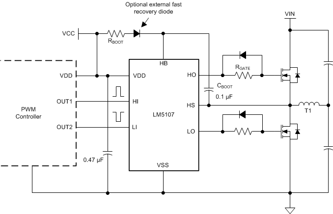
 Figure 16. LM5107 Driving MOSFETs in Half-Bridge Configuration
8.2.1 Design Requirements
See Table 2 for the parameter and values.
Table 2. Operating Parameters
| PARAMETER | VALUE |
|---|---|
| Gate Driver | LM5107 |
| MOSFET | CSD18531Q5A |
| VDD | 10 V |
| Qgmax | 43 nC |
| Fsw | 100 kHz |
| Dmax | 95% |
| IHBS | 10 µA |
| VDH | 1.0 V |
| VHBR | 7.1 V |
| VHBH | 0.4 V |
8.2.2 Detailed Design Procedure
8.2.2.1 Select Bootstrap and VDD capacitor
The bootstrap capacitor must maintain the HB pin voltage above the UVLO voltage for the HB circuit in any circumstances during normal operation. Calculate the maximum allowable drop across the bootstrap capacitor with Equation 1.
where
- VDD = Supply voltage of the gate drive IC
- VDH = Bootstrap diode forward voltage drop
- VHBL = VHBR – VHBH = 6.7 V, HB falling threshold
The quiescent current of the bootstrap circuit is 10 µA, which is negligible compared to the Qgs of the MOSFET
(see Equation 2 and Equation 3).


In practice the value for the CBOOT capacitor should be greater than that calculated to allow for situations where the power stage may skip pulse due to load transients. It is recommended to place the bootstrap capacitor as close to the HB and HS pins as possible.
As a general rule the local VDD bypass capacitor should be 10 times greater than the value of CBOOT.
The bootstrap and bias capacitors should be ceramic types with X7R dielectric. The voltage rating should be twice that of the maximum VDD to allow for loss of capacitance once the devices have a DC bias voltage across them and to ensure long-term reliability of the devices.
8.2.2.2 Select External Bootstrap Diode and Resistor
The bootstrap capacitor is charged by the VDD through the internal bootstrap diode every cycle when low side MOSFET turns on. The charging of the capacitor involves high peak currents, and therefore transient power dissipation in the internal bootstrap diode may be significant and dependent on its forward voltage drop. Both the diode conduction losses and reverse recovery losses contribute to the total losses in the gate driver and need to be considered in the gate driver IC power dissipation.
For high frequency and high capacitive loads, it may be necessary to consider using an external bootstrap diode placed in parallel with internal bootstrap diode to reduce power dissipation of the driver.
Bootstrap resistor RBOOT is selected to reduce the inrush current in DBOOT and limit the ramp up slew rate of voltage of HB-HS. It is recommended that RBOOT is between 2 Ω and 10 Ω. For this design, a current limiting resistor of 2.2 Ω is selected to limit inrush current of bootstrap diode.

8.2.2.3 Select Gate Driver Resistor
Resistor RGATE is sized to reduce ringing caused by parasitic inductances and capacitances and also to limit the current coming out of the gate driver. For this design 7.5-Ω resistors were selected for this design. Maximum HO and LO drive current are calculated by Equation 7 through Equation 10.


where
- IHOH = Maximum HO source current
- ILOH = Maximum LO source current
- IHOL = Maximum HO sink current
- ILOH = Maximum HO sink current
- VOH = High-Level output voltage drop across HB to HO or VDD to LO
- VOL = Low-Level output voltage drop across HO to HS or LO to GND
8.2.3 Power Dissipation
Power dissipation of the gate driver has two portions as shown in Equation 11.
Use Equation 12 to calculate the DC portion of the power dissipation (PDC).
where
- IQ is the quiescent current for the driver.
The quiescent current is the current consumed by the device to bias all internal circuits such as input stage, reference voltage, logic circuits, protections, and also any current associated with switching of internal devices when the driver output changes state (such as charging and discharging of parasitic capacitances, parasitic shoot-through, and so forth). The power dissipated in the gate-driver package during switching (PSW) depends on the following factors:
- Gate charge required of the power device (usually a function of the drive voltage VG, which is very close to input bias supply voltage VDD)
- Switching frequency
- Use of external gate resistors. When a driver device is tested with a discrete, capacitive load calculating the power that is required from the bias supply is fairly simple. The energy that must be transferred from the bias supply to charge the capacitor is given by Equation 13.
- CLOAD is load capacitor
- VDD is bias voltage feeding the driver
where
There is an equal amount of energy dissipated when the capacitor is charged and when it is discharged. This leads to a total power loss given by Equation 14.
where
- fSW is the switching frequency
The switching load presented by a power MOSFET is converted to an equivalent capacitance by examining the gate charge required to switch the device. This gate charge includes the effects of the input capacitance plus the added charge needed to swing the drain voltage of the power device as it switches between the ON and OFF states. Most manufacturers provide specifications of typical and maximum gate charge, in nC, to switch the device under specified conditions. Using the gate charge Qg, determine the power that must be dissipated when switching a capacitor which is calculated using the equation QG = CLOAD × VDD to provide Equation 15 for power.
This power PG is dissipated in the resistive elements of the circuit when the MOSFET is being turned on and off. Half of the total power is dissipated when the load capacitor is charged during turnon, and the other half is dissipated when the load capacitor is discharged during turnoff. When no external gate resistor is employed between the driver and MOSFET, this power is completely dissipated inside the driver package. With the use of external gate-drive resistors, the power dissipation is shared between the internal resistance of driver and external gate resistor.
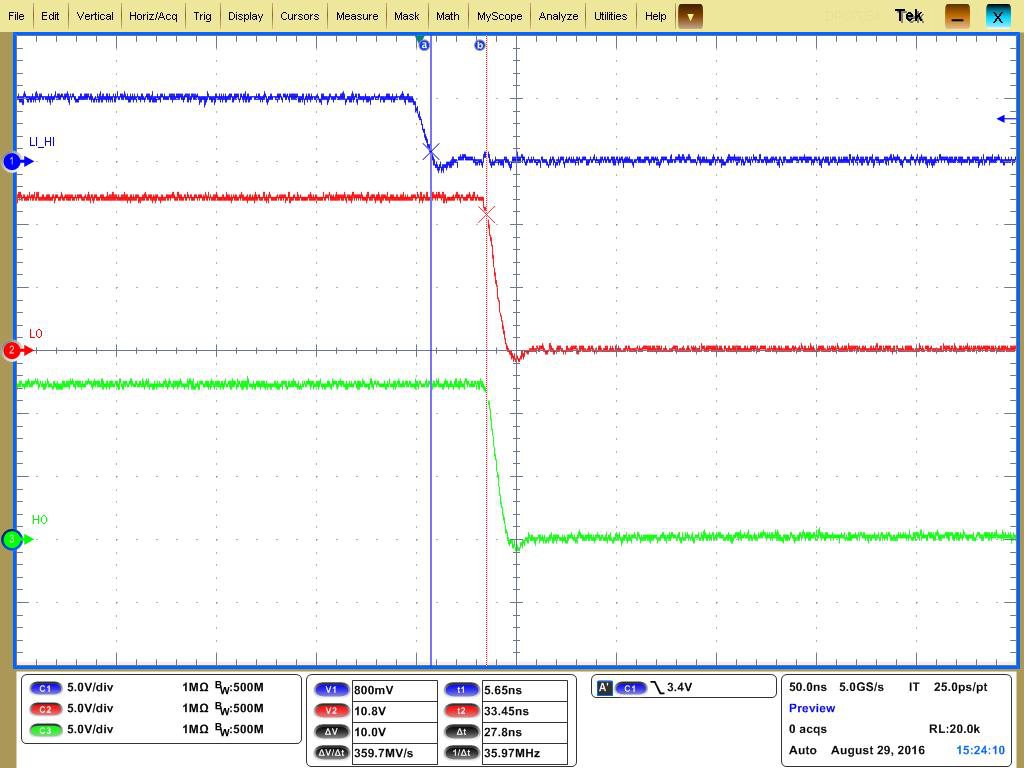
8.2.4 Application Curves

